Chip Antenna

a chip antenna and antenna technology, applied in the field of antennas, can solve the problems of not meeting the characteristic requirements of the new generation, conventional chip antennas, and small size, and achieve the effects of high manufacturing cost, high manufacturing process, and high cos

Inactive Publication Date: 2007-10-18
NAT TAIWAN UNIV OF SCI & TECH
View PDF11 Cites 57 Cited by
  • Summary
  • Abstract
  • Description
  • Claims
  • Application Information

AI Technical Summary

Benefits of technology

[0016] The conventional chip antennas function inefficiently. Moreover, the manufacturing process of the LTCC process is complicated and the cost thereof is very high, whose main drawbacks are the limited choices of the materials of conductive lines and ceramic substrate caused by the requirement of cofiring procedures, and the possible deformation of meandered lines caused by the sintered shrinkage of the ceramic substrates. Similar to those encountered in the complicated LTCC process, the drawbacks of most commercial chip antenna include high manufacturing cost, low freedom for radiation line design, long period and high cost for developing a product, and inefficient production.
[0017] It is therefore an objective of the present invention to provide a chip antenna, in which multiple meandered lines are designed with a single feed, which are folded into a three-dimensional antenna structure, to enhance the freedom of design and the performance of the three-dimensional antenna.
[0018] It is another objective of the present invention to provide a chip antenna, in which the composite of a polymer and ceramic material encloses the meandered lines of the antenna body, to mitigate the firing shrinking of the ceramic substrate as well as the deformation of the lines during the prior LTCC process.

Problems solved by technology

Due to the modern electronic devices becoming lightweight, and small and thin in size, conventional antennas, like rod antennas, Yaki antennas, dish antennas and so on, no longer fill the characteristic requirements of new generation.
But the conventional chip antenna still has some drawbacks, such as a slightly large size, insufficient efficiency, and high manufacturing cost.
However, the chip antenna with a flat metal line does not substantially decrease the size or enhance the efficiency thereof.
However, the radiation line of the antenna is a simple, flat, meandered line, such as a simple L-shaped or U-shaped meandered line, which cannot effectively decrease the size of the antenna.
Moreover, the antenna is a single meandered line with one single input port, the frequency band and bandwidth of which have a poor performance, and the antenna cannot be designed for antenna patterns with different polarizing directions.
The applications of the antenna are thus restricted and cannot match varied situations.
The ceramic material can be used to minimize the size of the antenna due to its high dielectric constant, but the LTCC process is very complicated.
Therefore, the three-dimensional antenna is composed of several flat, meandered lines, and is not easily designed for antenna patterns having a polarizing direction perpendicular to the substrate.
In addition, the dielectric constant of the ceramic material usually is limited due to very few materials being suitable for the LTCC process, and the prior art therefore cannot use a ceramic material with a suitable dielectric constant according to different characteristic requirements.
Because the LTCC process is applied, the manufacturing method of the antenna is very complicated and the cost thereof is also very high.
Moreover, the dielectric constant of the ceramic material usually is limited due to very few materials being suitable to the LTCC process, and the prior art therefore cannot choose the ceramic material with a suitable dielectric constant according to different characteristic requirements.
In addition, the three-dimensional antenna is a horizontal and spiral antenna, and therefore it is not easily designed for the antenna patterns having polarizing direction perpendicular to the substrate.
The conventional chip antennas function inefficiently.
Moreover, the manufacturing process of the LTCC process is complicated and the cost thereof is very high, whose main drawbacks are the limited choices of the materials of conductive lines and ceramic substrate caused by the requirement of cofiring procedures, and the possible deformation of meandered lines caused by the sintered shrinkage of the ceramic substrates.
Similar to those encountered in the complicated LTCC process, the drawbacks of most commercial chip antenna include high manufacturing cost, low freedom for radiation line design, long period and high cost for developing a product, and inefficient production.

Method used


Image

  • Chip Antenna
  • Chip Antenna
  • Chip Antenna

Examples


first embodiment

The First Embodiment

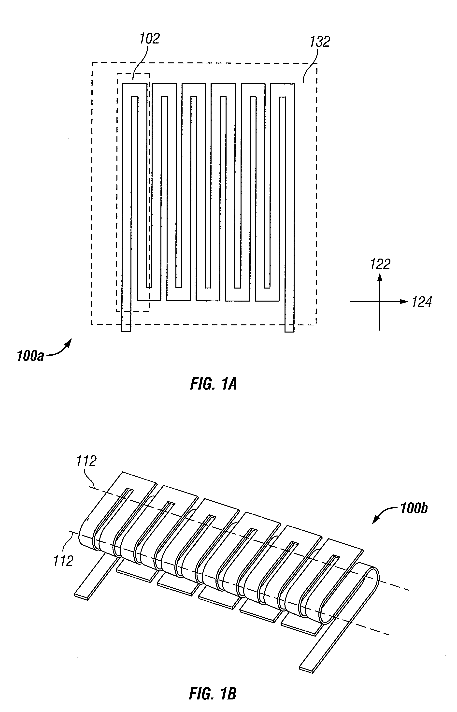
[0048]FIG. 1A illustrates a schematic view of a flat antenna body of the first embodiment of the invention, and FIG. 1B illustrates a schematic view of a three-dimensional antenna body formed by folding the flat antenna body in FIG. 1A. As illustrated in FIG. 1A, a flat antenna body 100a comprises multiple meandered lines 102 arranged in a direction 124, and the meandered lines 102 are electrically connected in series to form a meandered line set 132. The meandered line set 132 can be formed by punching a conductive sheet, such as continuously punching a copper sheet, or by etching a conductive sheet.

[0049] Next, the meandered line set 132 is folded in a direction perpendicular to the direction 124, i.e. the direction 122. As illustrated in FIG. 1B, the meandered line set 132 is folded with respect to a folding line 112, thus forming a three-dimensional antenna body 100b. The three-dimensional antenna body 160b is a horizontal antenna structure, which is thin, t...

second embodiment

The Second Embodiment

[0050] The second embodiment explains another three-dimensional antenna body, in which the folding direction thereof is different from that of the first embodiment.

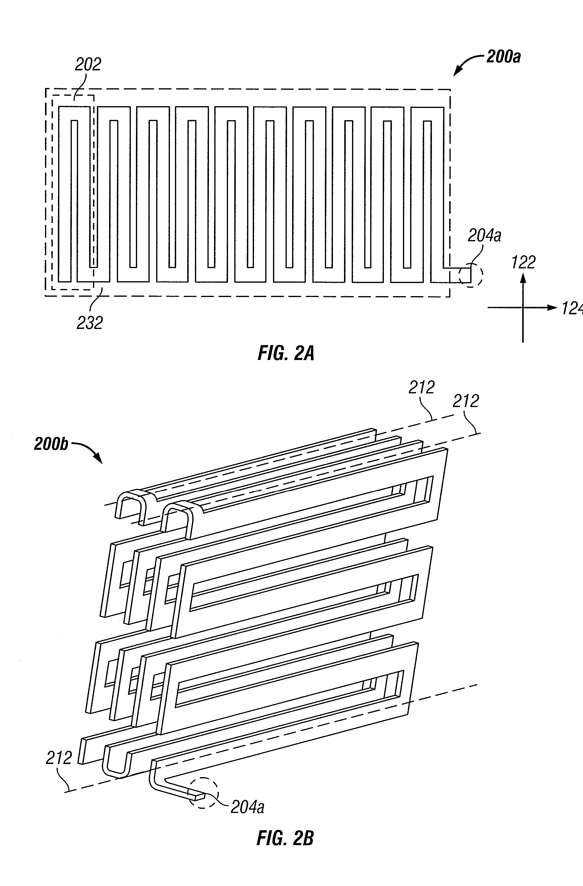
[0051]FIG. 2A illustrates a schematic view of a flat antenna body of the second embodiment of the invention, FIG. 2B illustrates a schematic view of a three-dimensional antenna body formed by folding the flat antenna body in FIG. 2A, and FIG. 2C illustrates a schematic view of a chip antenna formed by encapsulating the three-dimensional antenna body in FIG. 2B in a packaging material.

[0052] As illustrated in FIG. 2A, a flat antenna body 200a comprises multiple meandered lines 202 arranged in a direction 124, and the meandered lines 202 are electrically connected in series to form a meandered line set 232.

[0053] The major difference between the first and the second embodiments is their folding directions of their meandered lines, and thus, their radiating properties. In the second embodiment, the me...

third embodiment

The Third Embodiment

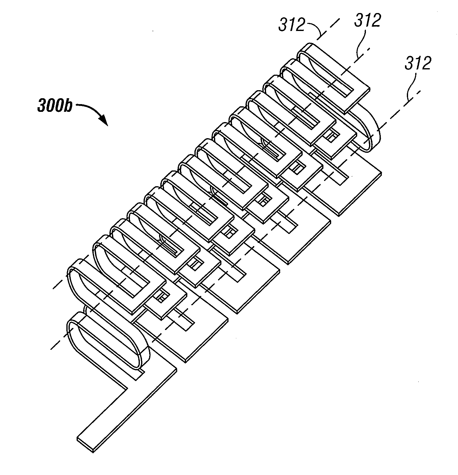
[0057] The third embodiment describes an antenna body with different sets of meandered lines. The meandered lines of different sets can be applied with different folding manners, such as folding lengths and angles, to form a three-dimensional antenna body.

[0058]FIG. 3A illustrates a schematic view of a flat antenna body of the third embodiment of the invention, and FIG. 3B illustrates a schematic view of a three-dimensional antenna body formed by folding the flat antenna body in FIG. 3A. As illustrated in FIG. 3A, a plurality of the first meandered lines 302 are arranged in a direction 122, and the first meandered lines 302 are electrically connected in series to form a first meandered line set 332. A plurality of the second meandered lines 304 are arranged in a direction 122, and the second meandered lines 304 are electrically connected in series to form a second meandered line set 334. The first meandered line set 332 and the second meandered line set 334 are ...


PUM


Abstract

A chip antenna has an antenna body and a package. The antenna body has multiple meandered metal lines and is encapsulated with the package. The material of the package is a dielectric composite formed with polymers and ceramic powders, which has a dielectric constant designed for the antenna. The characteristics of the chip antenna are determined by the structures of the antenna body and the dielectric constant of the package. Thus, a requirement for tiny structures in antenna applications can be satisfied.

Description

RELATED APPLICATIONS [0001] This application is a divisional of U.S. patent application Ser. No. 10 / 960,310 filed Oct. 06, 2004, which claims priority from, Taiwan Application Serial Number 92132453, filed Nov. 19, 2003, all of which are incorporated in its entirety by this reference thereto. BACKGROUND [0002] 1. Field of Invention [0003] The present invention relates to an antenna. More particularly, the present invention relates to a chip antenna. [0004] 2. Description of Related Art [0005] Many modern electronic devices, such as mobile telephones, computers, and network devices, are all provided with functions that communicate signals by wireless communications, following the great progress of the wireless communication science and technology. The main emitting and receiving devices used in wireless communication are signal transceivers and antennas configured thereon. Due to the modern electronic devices becoming lightweight, and small and thin in size, conventional antennas, li...

Claims


Application Information

Patent Timeline
Patent Type & Authority Applications(United States)
IPC IPC(8): H01Q1/36H01Q1/22H01Q1/24H01Q1/38
CPCH01Q1/22H01Q1/2283Y10T29/49018Y10T29/49016H01Q1/38
Inventor YANG, CHANG-FALI, JEN-HSUNCHEN, JING-MINGLIN, JUN-HONGLIN, SHUN-TIAN
Owner NAT TAIWAN UNIV OF SCI & TECH
Why Eureka
Try Eureka