Flat display panel and connection structure
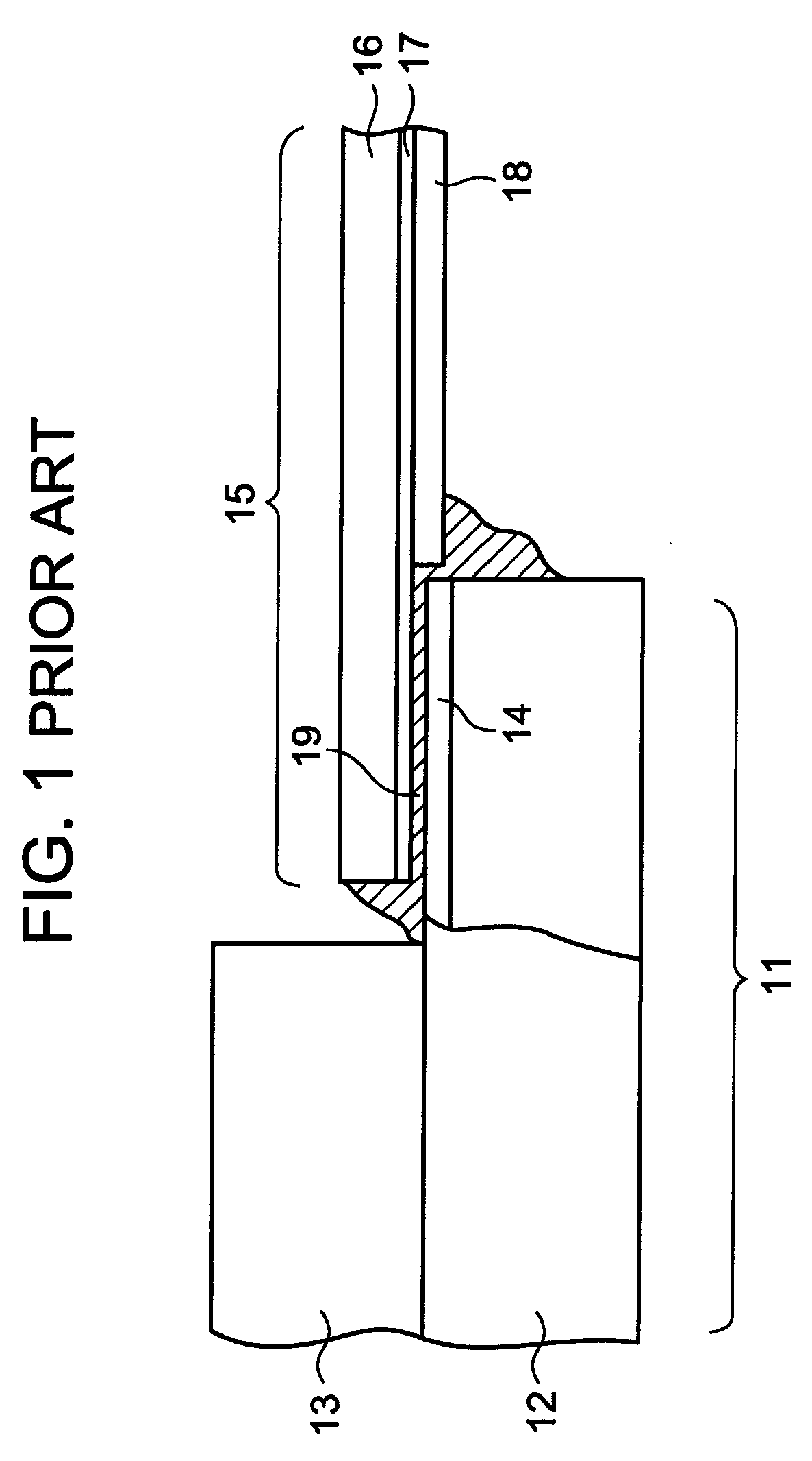
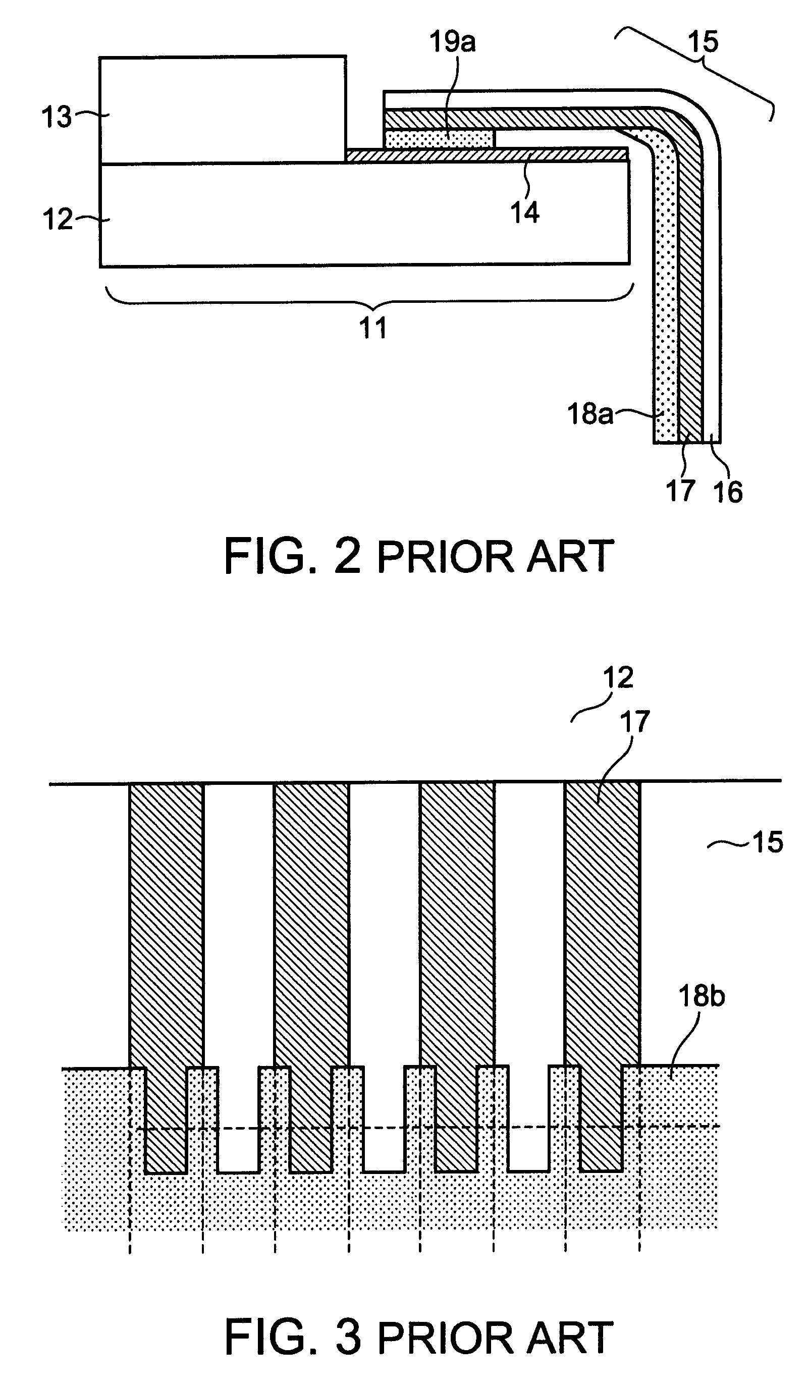
onnection structure technology, applied in the direction of coupling device connection, instruments, non-metallic protective coating application, etc., can solve the problem of not being able to not being able to completely prevent the possibility of short-circuit problem, and not being able to connect a panel and a flexible board in a flat panel display
- Summary
- Abstract
- Description
- Claims
- Application Information
AI Technical Summary
Benefits of technology
Problems solved by technology
Method used
Image
Examples
first embodiment
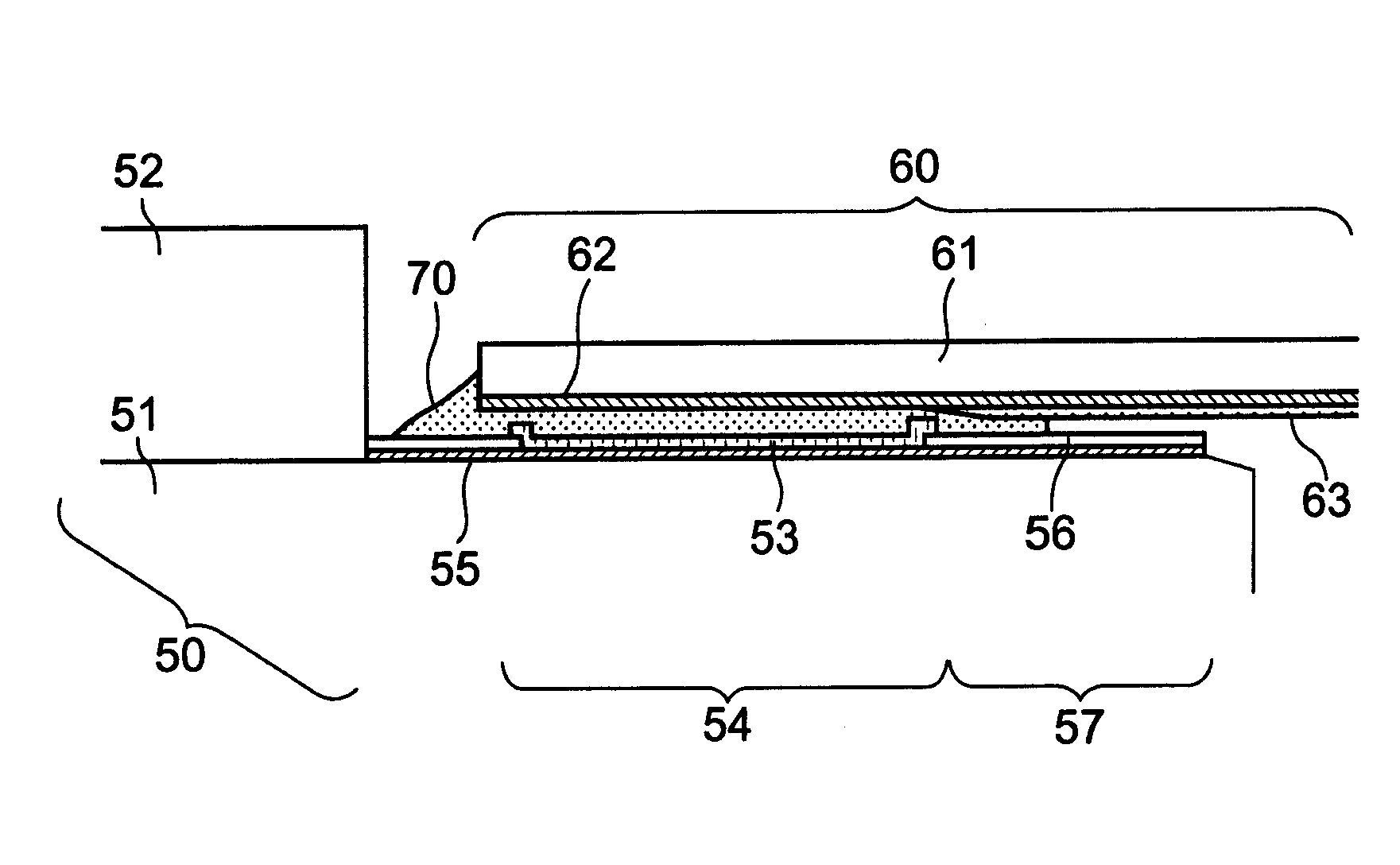
[0030]FIGS. 5A and 5B are a partial plan view and a partial cross sectional view, respectively, of a flat panel display (liquid-crystal display device) according to the present invention.
[0031]The liquid-crystal display device shown in these figures have an LCD panel 50 and a flexible board 60.
[0032]The LCD panel 50 has two glass boards, or a TFT board 51 and a color filter (CF) board 52. Pixel electrodes, scanning lines and signal lines (not shown) are formed on one surface of the TFT board 51. Color layers (not shown) assigned to the pixels are formed on one surface of the CF board 52.
[0033]The TFT board 51 and the CF board 52 are bonded together with a liquid-crystal layer interposed therebetween, and are sandwiched by a pair of polarizing plates (not shown).
[0034]The TFT board 51 has a greater size than the CF board 52, and the end face of the TFT board 51 projects out further than the end face of the CF board 52. A panel terminal electrode (for example, a transparent conductive...
second embodiment
[0052]the present invention will be described with reference to FIGS. 8A and 8B. In FIG. 8B, a base metal layer 55 is omitted.
[0053]In the second embodiment, a TCP (Tape Carrier Package) in place of the COF is used as a flexible board 60. The TCP has a base film 61 with a thickness of about 75 μm and hence has less flexibility in comparison with the COF. Therefore, the connection portion formed by the ACF 70 is stressed in the peeling direction due to the effect of the thickness of the solder resist 63, resulting in poor reliability. In other words, the connection between the panel terminal electrode 53 and the flexible board terminal electrode is adversely affected when the tip end of the solder resist 63 is located in the vicinity of the boundary between the valid connection region 54 and the non-connection region 57.
[0054]Therefore, according to the second embodiment, as shown in FIG. 8B, the tip end of the solder resist 63 is located closer to the panel end face relative to the ...
PUM
 Abstract
Description
Claims
Application Information


