Development device, process cartridge, and image forming apparatus
- Summary
- Abstract
- Description
- Claims
- Application Information
AI Technical Summary
Benefits of technology
Problems solved by technology
Method used
Image

Examples
first embodiment
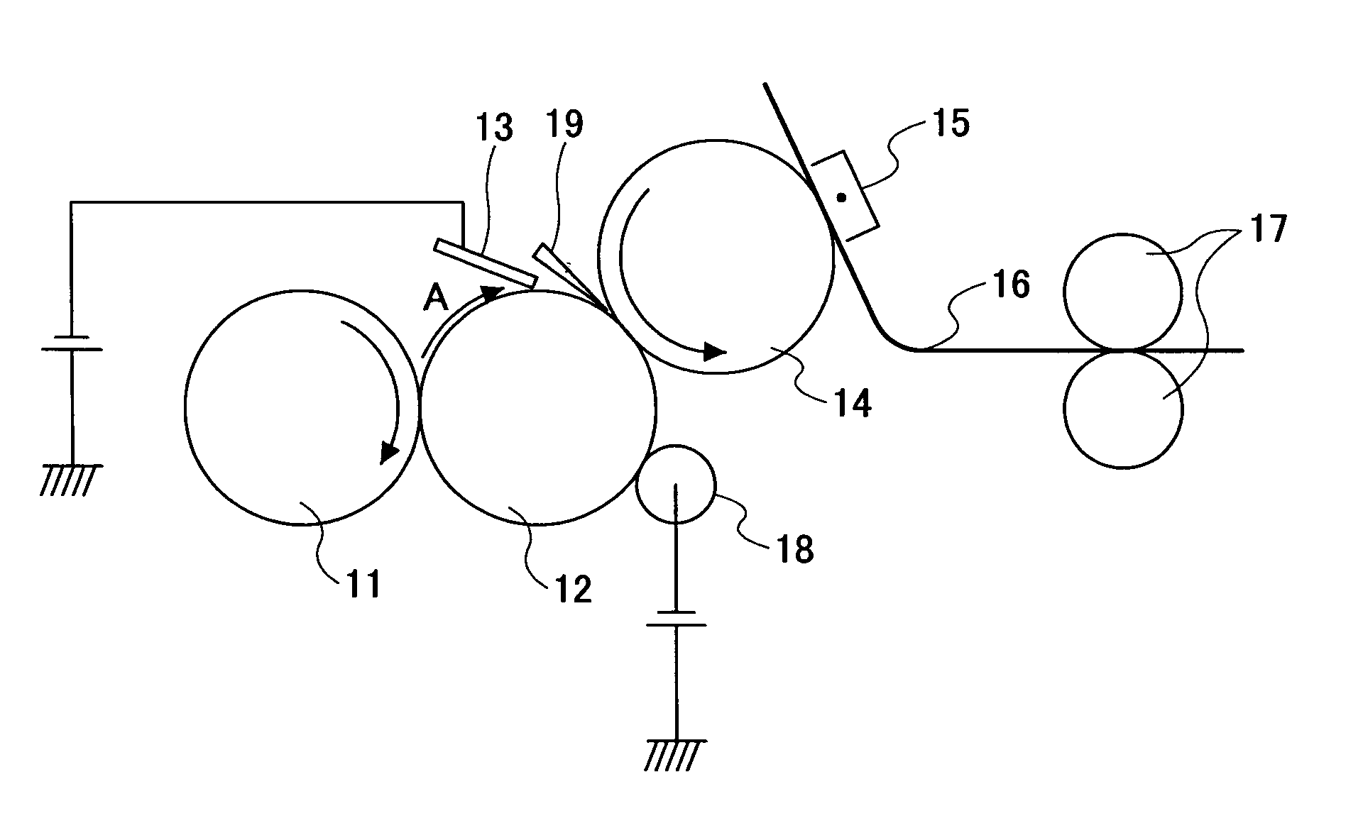
[0070]FIG. 1 is a schematic cross-sectional view showing a development device according to the present invention. In FIG. 1, a toner supply unit 11 carries changed toner and the toner is brought close to a closest portion of a conveying member 12. An electric field is formed between the toner supply unit 11 and the conveying member 12 and the toner is trapped in a conveying electric field formed on the conveying member 12 from electrostatic force received by the toner. The conveying member 12 has a three-phase electrode and is capable of conveying the charged toner by applying a conveying voltage of square waves while successively changing the conveying voltage. When the toner is conveyed, the toner forms what is called a cloud layer and moves in a direction indicated by arrow A in FIG. 1. Then, according to a development device 10 of the present embodiment, a uniform hopping height adjusting member 13 is disposed such that a predetermined gap is set between a surface of the conveyi...
second embodiment
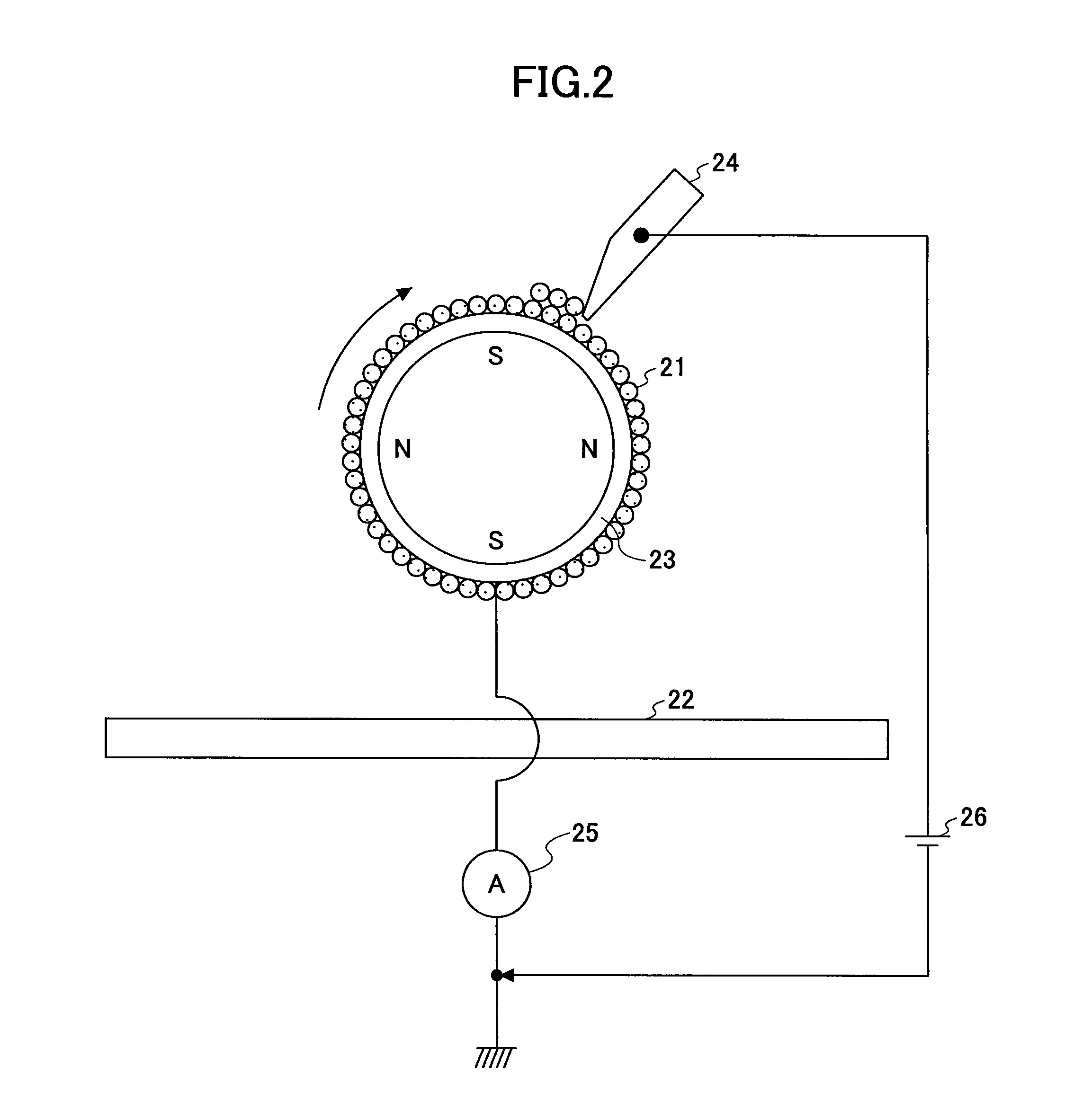
[0122] The following describes the present invention. As shown in FIG. 23, aluminum is deposited on a glass base 121 and an electrode pattern 122 is formed in which plural electrodes 122-1, 122-2, 122-3 . . . are arranged in the movement direction at a pitch of p [μm]. On the electrode pattern 122, a protection layer 123 coated with resin having a thickness of about 3 [μm] and volume resistivity of about 1010 [Ω·cm] is formed, thereby constructing a base 124. A charged toner layer 125 is formed on the base 124.
[0123] The charged toner layer 125 is formed by developing a solid image into a thin layer on the base 124 using a two-component development unit not shown in the drawings. The toner used in this case is polyester having a particle diameter of about 6 [μm] and a toner charge amount of about −22 [μC / g] when formed on the base 124 into the thin layer. As shown in FIG. 24, while an alternating voltage is applied from an alternating-current power supply 126 to an odd number electr...
third embodiment
[0158]FIG. 37A is a diagram showing a structure of a development device according to the present invention. As shown in FIG. 37A, plural perpendicular direction conveying electrodes 111 are arranged in an orthogonal direction relative to the conveying electrodes 101 of the conveying member 12 and at regular intervals in a width direction of the perpendicular direction conveying electrodes 111. Further, as shown in FIG. 37B which is a cross-sectional view taken along line E-E′ in FIG. 37A and in FIG. 37C which is a cross-sectional view taken along line F-F′ in FIG. 37A, on an insulating layer 110 laminated so as to cover the conveying electrodes 101 arranged on the support base 104, the perpendicular direction conveying electrodes 111 are arranged in the orthogonal direction relative to the conveying electrodes 101 and at regular intervals in the width direction and a surface protection layer 112 is laminated on the perpendicular direction conveying electrodes 111. In this manner, th...
PUM
 Abstract
Description
Claims
Application Information
 - R&D Engineer
- R&D Manager
- IP Professional
- Industry Leading Data Capabilities
- Powerful AI technology
- Patent DNA Extraction
Browse by: Latest US Patents, China's latest patents, Technical Efficacy Thesaurus, Application Domain, Technology Topic.
© 2024 PatSnap. All rights reserved.Legal|Privacy policy|Modern Slavery Act Transparency Statement|Sitemap