Semiconductor device having a recess channel transistor

a technology of semiconductor devices and transistors, which is applied in the field of memory devices, can solve the problems of degrading the refresh characteristics of dram structures and difficult to obtain proper refresh characteristics of devices, and achieve the effect of increasing the channel area

Inactive Publication Date: 2007-11-01
SK HYNIX INC
View PDF7 Cites 13 Cited by
  • Summary
  • Abstract
  • Description
  • Claims
  • Application Information

AI Technical Summary

Benefits of technology

[0010]Embodiments of the present invention are directed to a semiconductor device having a recess channel transistor with an increased channel area. According to one embodiment, the recess channel transistor is provided with a recess channel region including a vertical Silicon-on-Insulator (“SOI”) channel structure.

Problems solved by technology

This results in degradation of the refresh characteristics of a DRAM structure.
Accordingly, it is difficult to obtain proper refresh characteristics of the device due to the increased leakage current.

Method used


Image

  • Semiconductor device having a recess channel transistor
  • Semiconductor device having a recess channel transistor
  • Semiconductor device having a recess channel transistor

Examples


Embodiment Construction

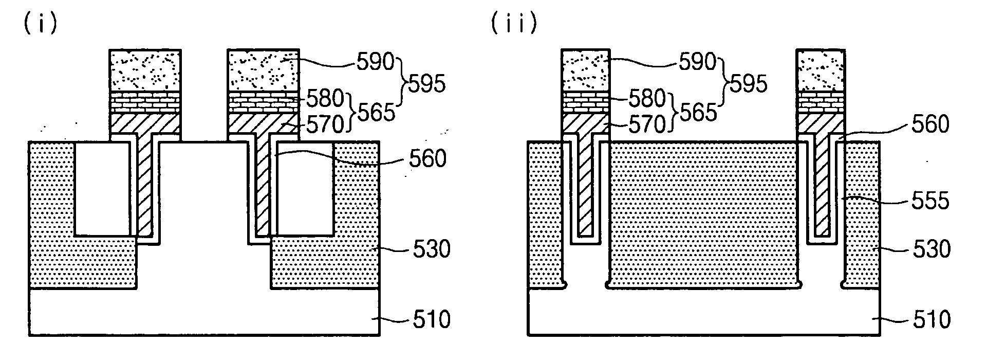
[0020]The present invention relates to semiconductor devices having a recess channel transistor with a recess channel region including a vertical SOI channel structure. The recess channel transistor has an active region having a recess region at a lower part of sidewalls of the active region, a recess channel region that has the vertical SOI channel structure formed at a sidewall of the device isolation structure in a longitudinal direction of a gate region, and a gate structure that fills the recess channel region. Accordingly, the recess channel transistor provides significantly improved refresh characteristics due to reducing leakage current flowing from storage nodes to body of the semiconductor substrate and improved short channel effect (“SCE”) because of a sufficiently securing channel area.

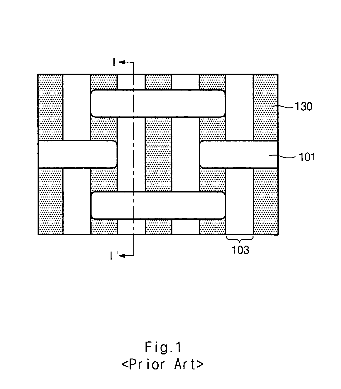
[0021]FIG. 4 is a simplified layout of a semiconductor device according to one embodiment of the present invention. The semiconductor device includes an active region 401 and a gate region...


PUM


Abstract

The semiconductor device having a recess channel transistor includes a device isolation structure formed in a semiconductor substrate to define an active region having a recess region at a lower part of sidewalls thereof and a recess channel region formed in the semiconductor substrate under the active region. A method for fabricating the semiconductor device includes forming a device isolation structure in a semiconductor substrate to form an active region having a recess region at a lower part of sidewalls thereof, a gate insulating film formed over the semiconductor substrate including the recess channel region, and a gate electrode formed over the gate insulating film to fill up the recess channel region.

Description

CROSS-REFERENCES TO RELATED APPLICATIONS[0001]The present application claims priority to Korean patent application number 10-2006-0038825, filed on Apr. 28, 2006, which is incorporated by reference in its entirety.BACKGROUND OF THE INVENTION[0002]The present invention relates to a memory device. More particularly, the present invention relates to a semiconductor device having a recess channel region including a vertical Silicon-on-Insulator (“SOI”) channel structure and a method for fabricating the same.[0003]When a channel length of a cell transistor is decreased, ion concentration of a cell channel region is generally increased in order to maintain the threshold voltage of the cell transistor. An electric field in source / drain regions of the cell transistor is enhanced to increase leakage current. This results in degradation of the refresh characteristics of a DRAM structure. Therefore, there is a need for semiconductor devices in which the refresh characteristics are improved.[00...

Claims


Application Information

Patent Timeline
Patent Type & Authority Applications(United States)
IPC IPC(8): H01L29/94
CPCH01L29/66621H01L27/10876H10B12/053H01L29/4236
Inventor CHUNG, SUNG WOONGLEE, SANG DON
Owner SK HYNIX INC
Why Eureka
Try Eureka