Electroluminescent devices including organic EIL layer

a technology of electroluminescent devices and electron injection layers, which is applied in the direction of organic semiconductor devices, discharge tube luminescnet screens, natural mineral layered products, etc., can solve the problems of large efficiency loss, performance limitations, and many desirable applications, and achieve improved electroluminescent features, reduced operational voltage, and high luminous efficiency

Inactive Publication Date: 2007-11-01
GLOBAL OLED TECH
View PDF17 Cites 161 Cited by
  • Summary
  • Abstract
  • Description
  • Claims
  • Application Information

AI Technical Summary

Benefits of technology

[0012] The device of the invention exhibit provides improved electroluminescent features such as reduced operational voltage and high luminous efficiency.

Problems solved by technology

While organic electroluminescent (EL) devices have been known for over two decades, their performance limitations have represented a barrier to many desirable applications.
However, it is generally believed that only 25% of the excitons created in an EL device are singlet excitons.
This results in a large loss in efficiency since 75% of the excitons are not used in the light emission process.

Method used


Image

  • Electroluminescent devices including organic EIL layer
  • Electroluminescent devices including organic EIL layer
  • Electroluminescent devices including organic EIL layer

Examples


examples

[0346] The invention and its advantages can be better appreciated by the following examples.

Device Examples 1-1 Through 1-6

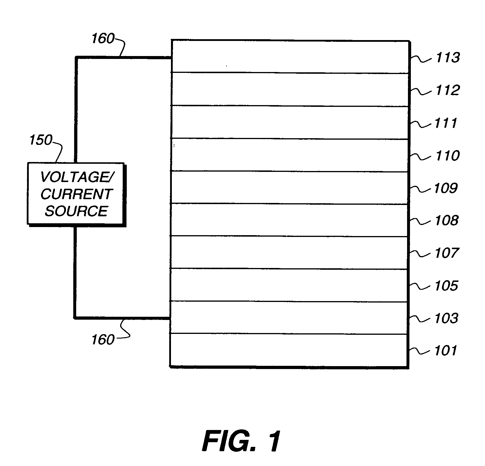
[0347] An EL device (Device 1-1) satisfying the requirements of the invention was constructed in the following manner: [0348] 1. A glass substrate, coated with an approximately 25 nm layer of indium-tin oxide (ITO) as the anode, was sequentially ultrasonicated in a commercial detergent, rinsed in deionized water, degreased in toluene vapor and exposed to an oxygen plasma for about 1 minute. [0349] 2. Over the ITO a 1 nm fluorocarbon (CFx) hole injecting layer (HIL) was deposited by plasma-assisted deposition of CHF3 as described in U.S. Pat. No. 6,208,075. [0350] 3. Next, a hole transporting layer (HTL) of N,N′-di-1-naphthyl-N,N′-diphenyl4,4′-diaminobiphenyl (NPB) was vacuum deposited to a thickness of 75 nm. [0351] 4. An exciton / electron blocking layer (EBL) of 4,4′,4″-tris(carbazolyl)-triphenylamine (TCTA) was vacuum deposited to a thickness of 10 nm. [0352]...


PUM

PropertyMeasurementUnit
LUMOaaaaaaaaaa
thicknessaaaaaaaaaa
thickaaaaaaaaaa

Abstract

An OLED device comprises a cathode, an anode, and has therebetween a light emitting layer (LEL) comprising a phosphorescent emitting compound disposed in a host comprising a mixture of at least one electron transporting co-host and at least one hole transporting co-host, wherein there is present an electron transporting layer contiguous to the LEL on the cathode side and wherein there is present an EIL layer containing a heteroaromatic compound contiguous to the cathode.

Description

CROSS-REFERENCE TO RELATED APPLICATION [0001] This application is cofiled as part of a group of five applications under attorney Docket Nos. 91082, 91926, 92030, 92055, and 92056.FIELD OF INVENTION [0002] This invention relates to organic electroluminescent (EL) devices. More specifically, this invention relates to phosphorescent devices including a electron injection layer. BACKGROUND OF THE INVENTION [0003] While organic electroluminescent (EL) devices have been known for over two decades, their performance limitations have represented a barrier to many desirable applications. In simplest form, an organic EL device is comprised of an anode for hole injection, a cathode for electron injection, and an organic medium sandwiched between these electrodes to support charge recombination that yields emission of light. These devices are also commonly referred to as organic light emitting diodes, or OLEDs. Representative of earlier organic EL devices are Gurnee et al. U.S. Pat. No. 3,172,8...

Claims


Application Information

Patent Timeline
Patent Type & Authority Applications(United States)
IPC IPC(8): H01L51/54
CPCH01L51/0058H01L51/0059H01L51/006H01L51/0067H01L51/0069H01L2251/5384H01L51/0081H01L51/0085H01L51/5016H01L51/5092H01L51/0072H10K85/626H10K85/631H10K85/633H10K85/654H10K85/656H10K85/324H10K85/342H10K85/6572H10K50/11H10K2101/10H10K50/171H10K2101/90H05B33/14C09K11/06H10K50/00
Inventor KONDAKOVA, MARINA E.KONDAKOV, DENIS Y.YOUNG, RALPH H.BROWN, CHRISTOPHER T.KLUBEK, KEVIN P.JARIKOV, VIKTOR V.ZUBERI, SHEENA
Owner GLOBAL OLED TECH
Why Eureka
Try Eureka