Process monitoring apparatus and method for monitoring process

a technology of process monitoring and process monitoring, which is applied in the direction of basic electric elements, semiconductor/solid-state device testing/measurement, instruments, etc., can solve the problems of reducing operating rates, affecting the accuracy of measurement results, so as to prevent unauthorised use and reduce operating rates

Inactive Publication Date: 2007-11-01
LG ELECTRONICS INC +1
View PDF12 Cites 2 Cited by
  • Summary
  • Abstract
  • Description
  • Claims
  • Application Information

AI Technical Summary

Benefits of technology

[0011] Furthermore, an unauthorized use can be prevented by storing a keyword in an Read Only Memory (ROM) of the process monitor.
[0013] Moreover, semiconductor manufacturing apparatus according to the present invention can compare the measured data read by the reader / writer with predetermined reference data and can control the manufacturing process in a predetermined way, if the measured data exceeds a predetermined range of the reference data.
[0014] The process monitor according to the present invention uses a capacitor as a power source. The capacitor can be hardly deteriorated and, therefore, there is no fear of contaminating a process chamber. Further, data for only a specific period of time can be obtained by using a timer. Further, unauthorized use can be prevented because a keyword is checked when reading data. The semiconductor manufacturing apparatus according to the present invention uses the process monitor to monitor the manufacturing process without fear of contamination or decrease in operating rates and indicates appropriate maintainance for the apparatus.

Problems solved by technology

If, at each time, measuring by inserting a probe or the like is carried out, the measurement is very troublesome and a wiring, for measurement and control is necessary, which causes a disturbance in a measuring object.
A simultaneous multipoint measurement is difficult and measurement at an area where the measurement is actually required is also difficult.
Furthermore, a problem of contamination or a problem of decrease in operating rates, arises.
However, a battery, which is a power supply source for the wafer sensor, is deteriorated by repeated charging and discharging.
A material of which the battery is made could contaminate a plasma processing chamber if the sensor wafer is broken by an unexpected accident or the like.

Method used


Image

  • Process monitoring apparatus and method for monitoring process
  • Process monitoring apparatus and method for monitoring process
  • Process monitoring apparatus and method for monitoring process

Examples


Embodiment Construction

[0019] Embodiments of this invention will be explained with reference to the drawings.

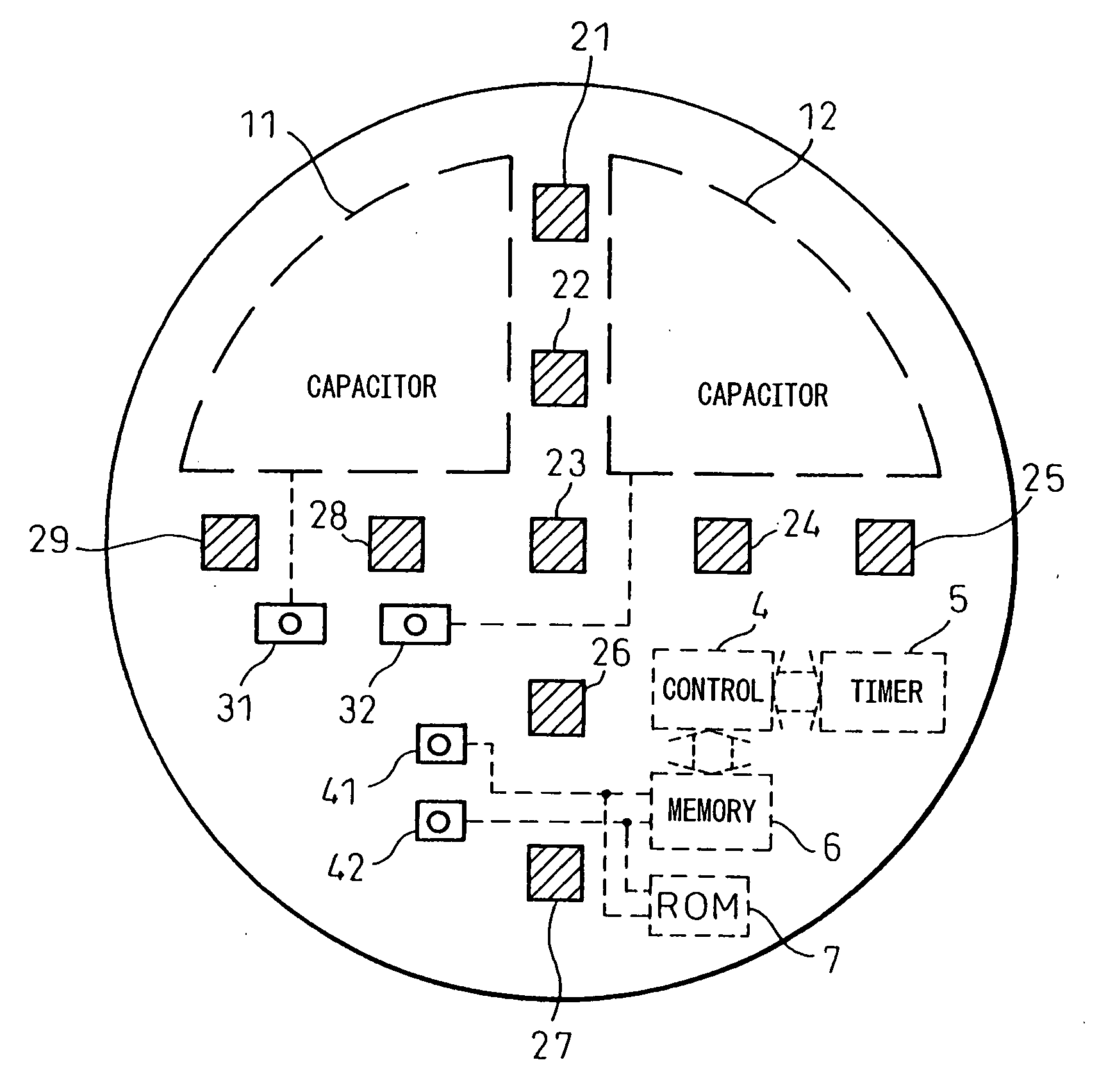
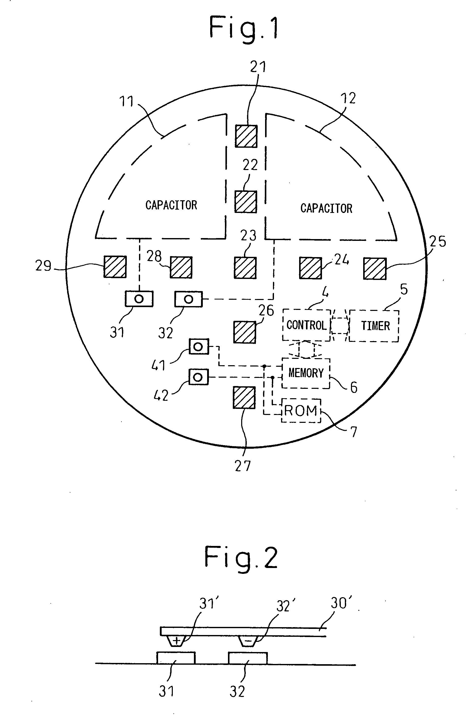
[0020]FIG. 1 is a schematic view of a process monitor according to an embodiment of this invention. The process monitor, in FIG. 1, is provided with nine sensors 21 to 29 each 10 mm square, arranged crosswise on a surface of a semiconductor wafer 1 having a diameter of, for example, 300 mm. In this embodiment, multilayer capacitors 11 and 12, which are connected in series to serve as a power source, are arranged at two places of the wafer 1 and are used as a power source for measurement by the sensors and reading the measured signals. The capacitors are charged and discharged through the charging and discharging terminals 31 and 32 connected with positive and negative electrodes of the capacitors. Whether the capacitors are connected in series or in parallel can be appropriately determined, in accordance with required capacity, withstand voltage or the like.

[0021] Furthermore, a timer 5 and a con...


PUM


Abstract

A sensor on a semiconductor wafer is used as a process monitor and a capacitor is employed as a power supply for the sensor. The capacitor can be formed by stacking a poly-silicon layer and a silicon nitride layer on the wafer. A timer can be used to specify an operation time or an operation timing, etc. Furthermore, unauthorized use is prevented by storing a keyword in an ROM of the process monitor.

Description

CROSS-REFERENCE TO RELATED APPLICATIONS [0001] This application is a division of U.S. patent application Ser. No. 10 / 532,991, filed Apr. 28, 2005, which is the National Phase of International Application PCT JP03 / 12555, filed Sep. 30, 2003, which claims priority to Japan Application No. 2002-318116, filed Oct. 21, 2002, the entire disclosures of which are incorporated herein by reference.BACKGROUND OF THE INVENTION [0002] 1. Field of the Invention [0003] The present invention relates to a process monitor for monitoring a semiconductor manufacturing process, such as a plasma process, and to a semiconductor manufacturing apparatus having a process monitor. [0004] 2. Prior Art [0005] Conventionally, in a semiconductor manufacturing apparatus, a measurement of a plasma density or a temperature, etc., to optimally control a plasma process is carried out, for example, by inserting a plasma probe or a thermocouple into a plasma processing chamber at a time of development in a factory. Howe...

Claims


Application Information

Patent Timeline
Patent Type & Authority Applications(United States)
IPC IPC(8): H01L21/00H01L21/205H01L21/66H01L21/3065H01L23/522
CPCH01L21/67253H01L23/5223H01L22/32H01L2924/0002H01L2924/00H01L21/3065H01L22/00
Inventor YUASA, MITSUHIRO
Owner LG ELECTRONICS INC
Why Eureka
Try Eureka