Analysis and optimization of manufacturing yield improvements

a technology of optimization and manufacturing yield, applied in the direction of cad circuit design, computer aided design, instruments, etc., can solve the problems of reducing the overall manufacturing yield of the circuit, affecting and becoming more difficult to manufacture, so as to reduce the likelihood of a defect occurring, and improve the design of the circuit.

Inactive Publication Date: 2007-11-01
MENTOR GRAPHICS CORP
View PDF5 Cites 25 Cited by
  • Summary
  • Abstract
  • Description
  • Claims
  • Application Information

AI Technical Summary

Benefits of technology

[0009] Advantageously, various examples of the invention provide techniques for improving the design of circuits, such as integrated microcircuits. With some implementations of the invention, a proposed circuit design is analyzed to identify design features associated with yield loss in manufactured circuits (that is, features associated the occurrence of defects during the manufacturing process). For example, the analysis may identify design features that have a significant probability of being improperly formed during a manufacturing process. Next, any design changes that will reduce the yield losses associated with the yield loss features are determined. That is, various changes to the circuit design are determined that, when implemented, will reduce or eliminate the likelihood of a defect occurring in a circuit manufactured from the design.

Problems solved by technology

As microcircuits become more complex, they also become more difficult to manufacture.
If a circuit device or connection is not properly formed during the manufacturing process, the microcircuit may operate incorrectly or even fail altogether.
A higher probability of a defect occurring in individual circuits will result in a lower overall manufacturing yield for the circuit.
The complexity of modern integrated circuits has led to a dramatic rise in the number of defects for these circuits, however.
At nanometer geometries, for example, these defects often occur only as a result of the interaction between the design and the process, rather than from a correctable deficiency in the manufacturing process itself.
It has therefore become increasingly difficult to increase manufacturing yield by changing the manufacturing process or equipment at the foundry.

Method used


Image

  • Analysis and optimization of manufacturing yield improvements
  • Analysis and optimization of manufacturing yield improvements
  • Analysis and optimization of manufacturing yield improvements

Examples


Embodiment Construction

Operating Environment

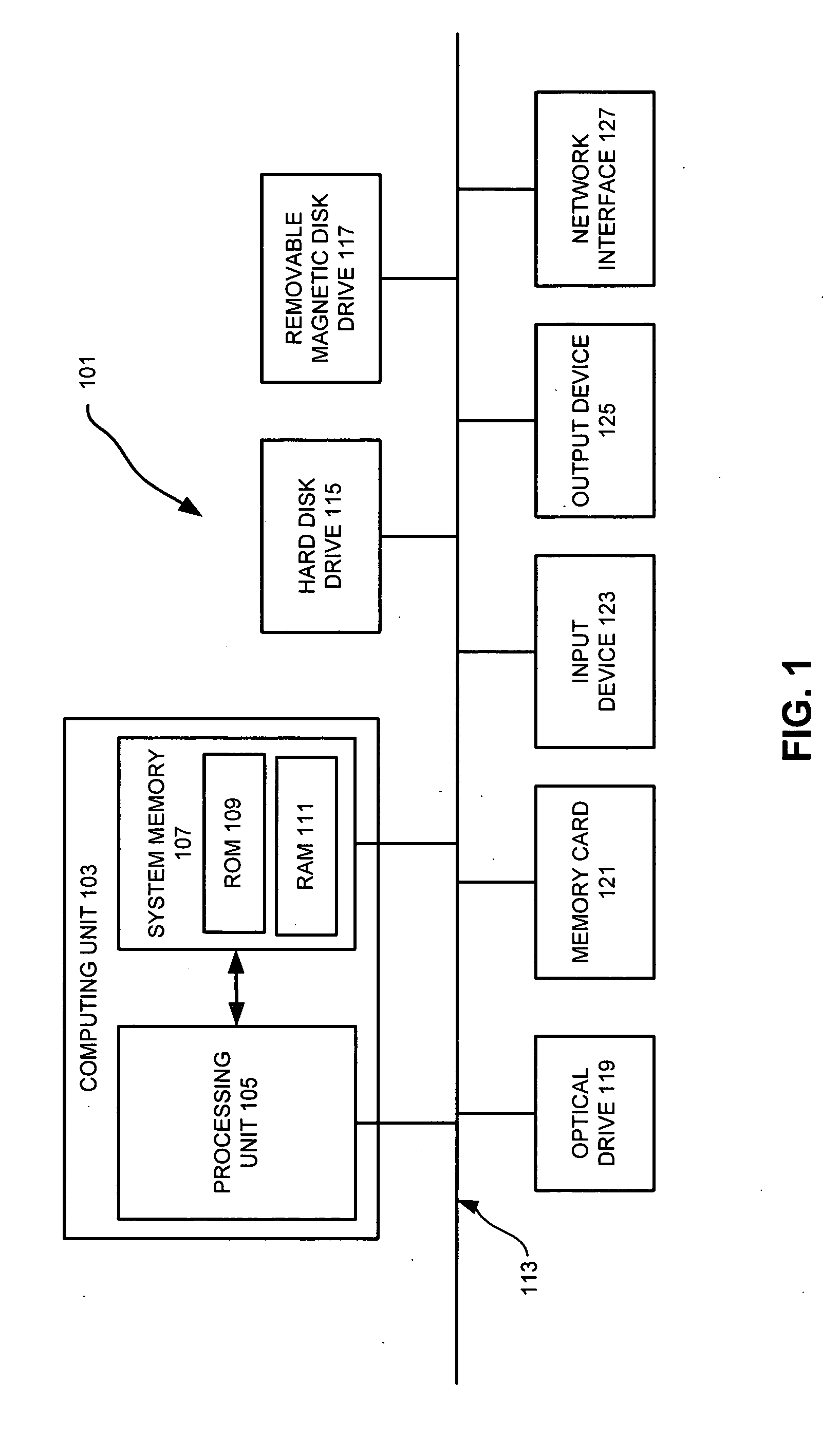
[0016] Various examples of the invention may be implemented through the execution of software instructions by a computing device, such as a programmable computer. Accordingly, FIG. 1 shows an illustrative example of a computing device 101. As seen in this figure, the computing device 101 includes a computing unit 103 with a processing unit 105 and a system memory 107. The processing unit 105 may be any type of programmable electronic device for executing software instructions, but will conventionally be a microprocessor. The system memory 107 may include both a read-only memory (ROM) 109 and a random access memory (RAM) 111. As will be appreciated by those of ordinary skill in the art, both the read-only memory (ROM) 109 and the random access memory (RAM) 111 may store software instructions for execution by the processing unit 105.

[0017] The processing unit 105 and the system memory 107 are connected, either directly or indirectly, through a bus 113 or altern...


PUM


Abstract

Techniques for improving the design of circuits, such as integrated microcircuits. A proposed circuit design is analyzed to identify design features associated with yield loss in manufactured circuits. Corrective design changes that will reduce the yield losses associated with the yield loss features then are designated. Once the corrective design changes have been determined, the corrective design changes that will optimize the manufacturing yield of the circuit are selected and incorporated into the circuit design. This analysis and revision process may then be repeated for each revised circuit design, until no further reduction in the manufacturing can be obtained.

Description

FIELD OF THE INVENTION [0001] The present invention relates to various techniques and tools to assist in the design of circuits, such as integrated circuits. Various aspects of the present invention are particularly applicable to selecting and implementing changes to a circuit design that will improve the yield of circuits manufactured from the design. BACKGROUND OF THE INVENTION [0002] Electronic circuits, such as integrated microcircuits, are used in a variety of products, from automobiles to microwaves to personal computers. Designing and fabricating microcircuit devices typically involves many steps, known as a “design flow.” The particular steps of a design flow are highly dependent upon the type of microcircuit, its complexity, the design team, and the microcircuit fabricator or foundry that will manufacture the microcircuit. Software and hardware “tools” then verify the design at various stages of the design flow by running software simulators and / or hardware emulators, and e...

Claims


Application Information

Patent Timeline
Patent Type & Authority Applications(United States)
IPC IPC(8): G06F17/50
CPCG06F17/5068G06F30/39
Inventor PIKUS, FEDOR G.LOBASSO, STEVEN WILLIAMALBRECHT, ROBIN KIRKSRINJVASAN, SRIDHAR
Owner MENTOR GRAPHICS CORP
Why Eureka
Try Eureka