Multilayer interconnect structure containing air gaps and method for making

a multi-layer interconnect and air gap technology, applied in the direction of electrical equipment, semiconductor devices, semiconductor/solid-state device details, etc., can solve the problems of affecting chip speed, and thus chip performance, metal wiring features are more susceptible to opening and shortening, and structures with air gaps may not be as uniformly planar

Active Publication Date: 2007-11-08
GLOBALFOUNDRIES US INC
View PDF9 Cites 51 Cited by
  • Summary
  • Abstract
  • Description
  • Claims
  • Application Information

AI Technical Summary

Benefits of technology

[0013] The present invention provides a reliable, high-performance multilayer interconnect structure containing air gaps. More particularly, th...

Problems solved by technology

By means of their effects on signal propagation delays, the materials and layout of these interconnect structures can substantially impact chip speed, and thus chip performance.
In addition, another concern with air gap dielectrics is that the dielectrics leave metal wiring features more susceptible to the opens and shorts induced by electromigration-driven mass tr...

Method used


Image

  • Multilayer interconnect structure containing air gaps and method for making
  • Multilayer interconnect structure containing air gaps and method for making
  • Multilayer interconnect structure containing air gaps and method for making

Examples


Embodiment Construction

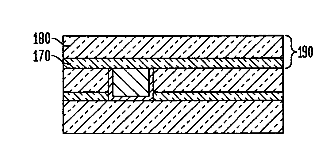
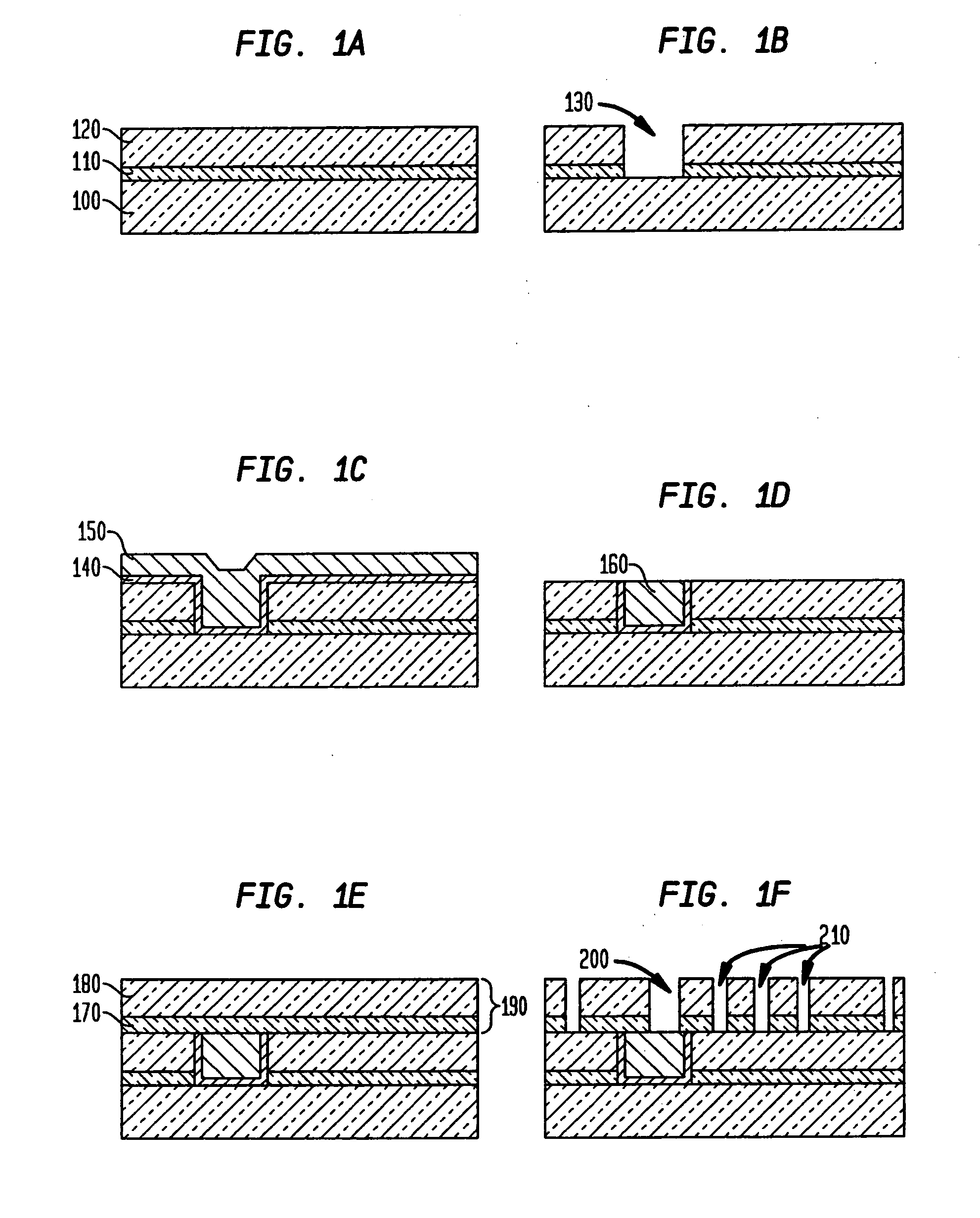
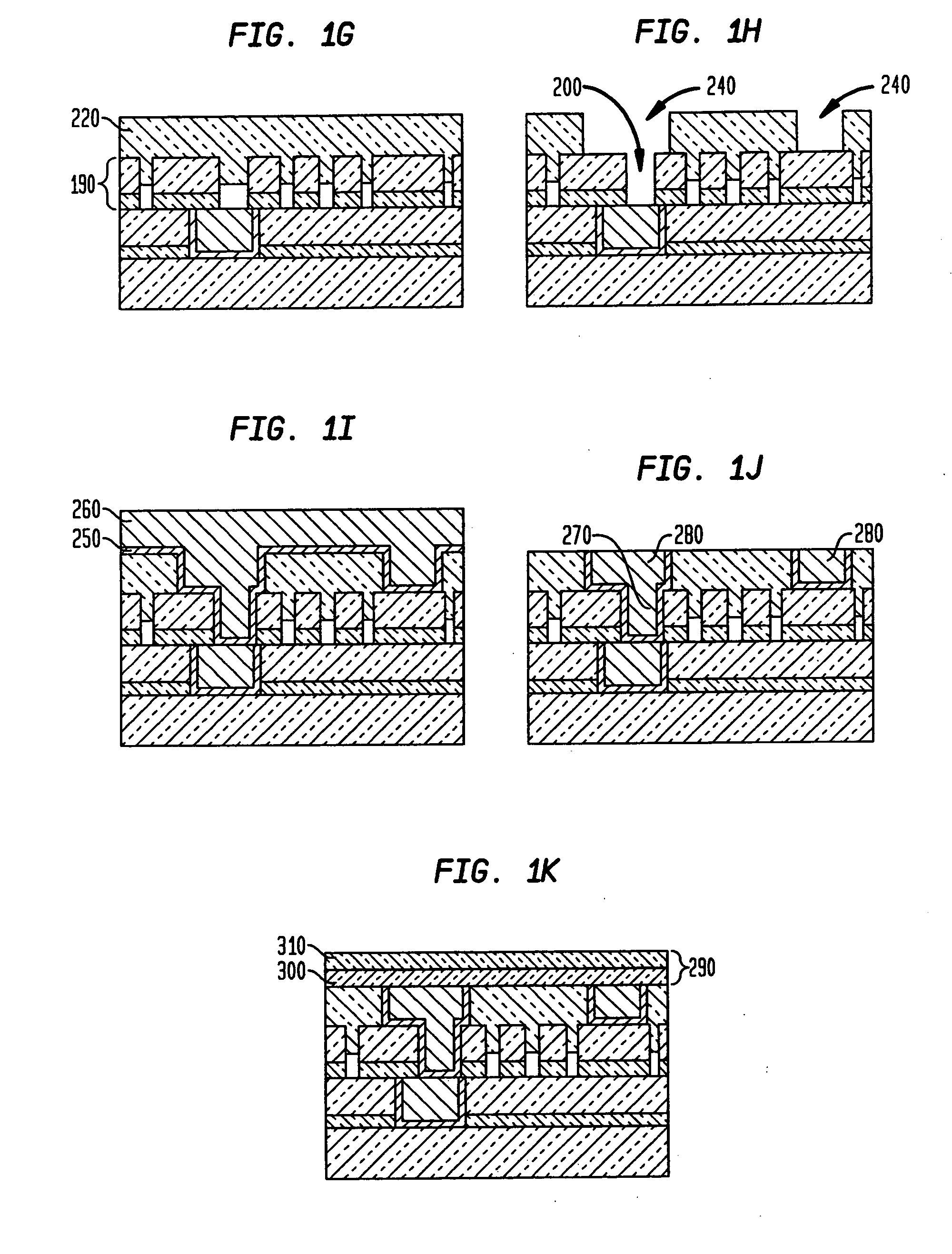
[0035] The present invention, which provides a high-performance multilayer interconnect structure containing air gaps, and a method of fabricating the same, will now be described in greater detail by referring to the following description and drawings that accompany the present application. It is noted that the drawings are provided for illustrative purposes, and as such, they are not drawn to scale. If not needed for understanding a particular drawing, reference numerals shown in a set of drawings are not repeated in subsequent drawings.

[0036] In the following description, numerous specific details are set forth, such as particular structures, components, materials, dimensions, processing steps and techniques, in order to provide a thorough understanding of the present invention. However, it will be appreciated by one of ordinary skill in the art that the invention may be practiced without these specific details. In other instances, well-known structures or processing steps have n...


PUM


Abstract

A multilevel air-gap-containing interconnect structure and a method of fabricating the same are provided. The multilevel air-gap-containing interconnect structure includes a collection of interspersed line levels and via levels, with via levels comprising conductive vias embedded in one or more dielectric layers in which the dielectric layers are solid underneath and above line features in adjacent levels, and perforated between line features. The line levels contain conductive lines and an air-gap-containing dielectric. A solid dielectric bridge layer, containing conductive contacts and formed by filling in a perforated dielectric layer, is disposed over the collection of interspersed line and via levels.

Description

CROSS REFERENCE TO RELATED APPLICATIONS [0001] Cross reference is made to U.S. application Ser. No. 09 / 374,839 filed Aug. 14, 1999 by L. Clevenger et al. entitled “Semi Sacrificial Diamond for Air Dielectric Formation” and to U.S. application Ser. No. 09 / 742,976 filed Dec. 20, 2000 by K. S. Petrarca et al. entitled “Microprocessor Having Air as a Dielectric and Encapsulated Lines, Process for Manufacture,” both directed to multilevel interconnect structures on integrated circuit chips incorporating a gaseous dielectric medium in at least one level, confined to within the chip by a dielectric encapsulant.FIELD OF THE INVENTION [0002] The present invention relates to air-gap-containing metal / insulator interconnect structures for Very Large Scale Integrated (VLSI) and Ultra Large Scale Integrated (ULSI) devices and packaging, and more particularly to structures, methods, and materials relating to the incorporation of air gaps into multiple levels of multilayer interconnect structures. ...

Claims


Application Information

Patent Timeline
IPC IPC(8): H01L21/4763
CPCH01L21/7682H01L21/76831H01L21/76835H01L23/5222H01L2924/0002H01L23/53295H01L2924/00H01L21/76808H01L2221/1026H01L2221/1031
Inventor JAHNES, CHRISTOPHER V.NITTA, SATYANARAYANA V.PETRARCA, KEVIN S.SAENGER, KATHERINE L.
Owner GLOBALFOUNDRIES US INC
Why Eureka
Try Eureka