Interconnect with multiple layers of conductive material with grain boundary between the layers

a technology of conductive material and interconnect structure, which is applied in the direction of basic electric elements, semiconductor/solid-state device manufacturing, electric apparatus, etc., can solve the problems of extruded metal lines, atom migration failure, and inability to withstand extrusion, so as to minimize the electromigration failure of such an interconnect structure, the effect of minimizing the migration of atoms and minimizing the electromigration failure of the via structur

Inactive Publication Date: 2006-02-21
ADVANCED MICRO DEVICES INC
View PDF2 Cites 2 Cited by
  • Summary
  • Abstract
  • Description
  • Claims
  • Application Information

AI Technical Summary

Benefits of technology

[0020]In this manner, the grain boundaries formed between a plurality of layers of conductive material act as shunt by-pass paths for migration of atoms of the conductive material to minimize migration of atoms of the conductive material along the interface between a dielectric passivation or capping layer and the interconnect structure. In turn, electromigration failure of such an interconnect structure is minimized. In addition, the grain boundaries formed between the plurality of layers of conductive material in a via structure minimize charge carrier wind-force along the direction of current flow through the via structure to further minimize electromigration failure of the via structure.

Problems solved by technology

However, as the width of metal lines are scaled down to smaller submicron and even nanometer dimensions, aluminum metallization shows electromigration failure.
Electromigration failure, which may lead to open and extruded metal lines, is now a commonly recognized problem.
Moreover, as dimensions of metal lines further decrease, metal line resistance increases substantially, and this increase in line resistance may adversely affect circuit performance.
Thus, copper may diffuse easily into these common integrated circuit materials to degrade the circuit performance of integrated circuits.

Method used


Image

  • Interconnect with multiple layers of conductive material with grain boundary between the layers
  • Interconnect with multiple layers of conductive material with grain boundary between the layers
  • Interconnect with multiple layers of conductive material with grain boundary between the layers

Examples


Embodiment Construction

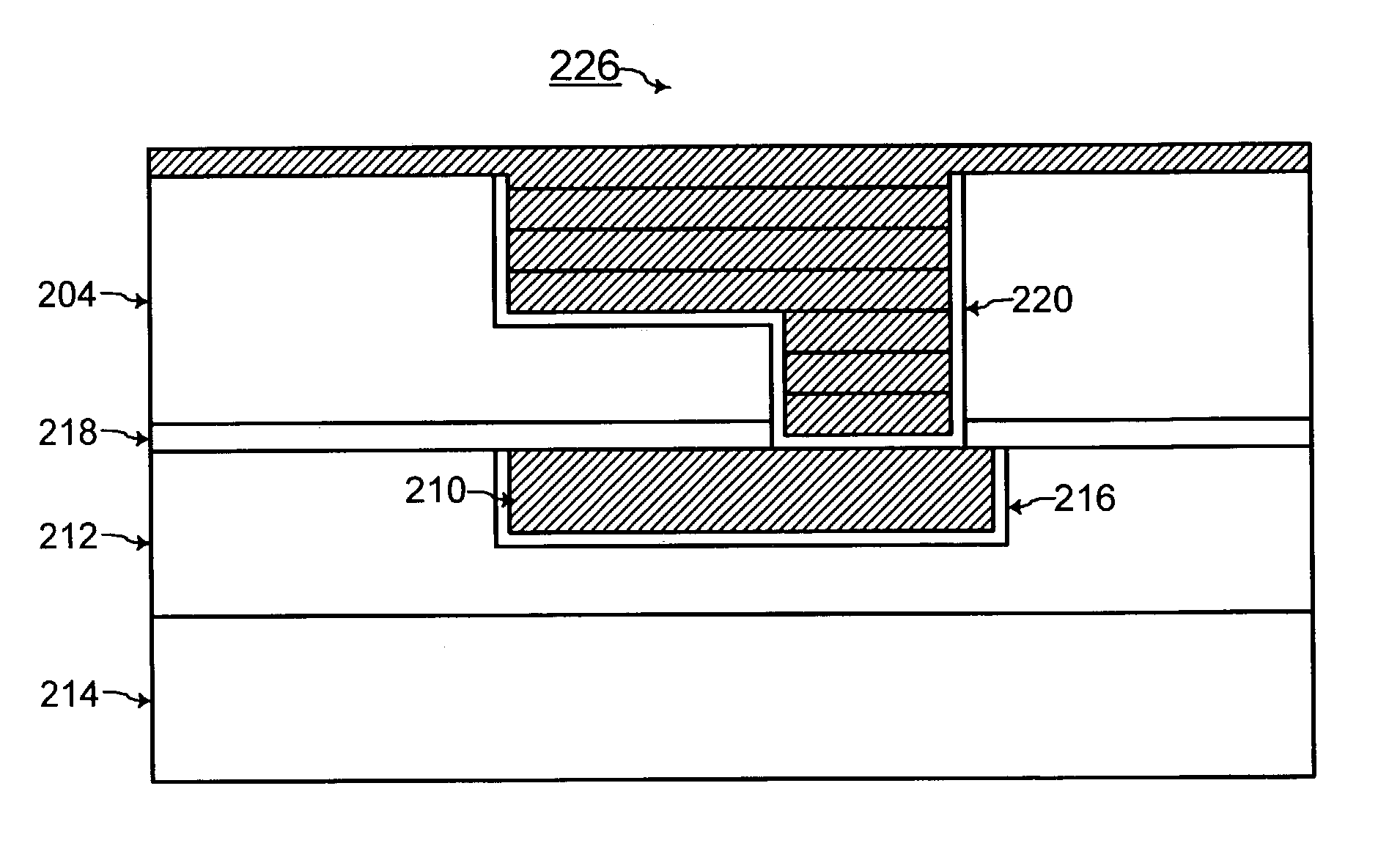
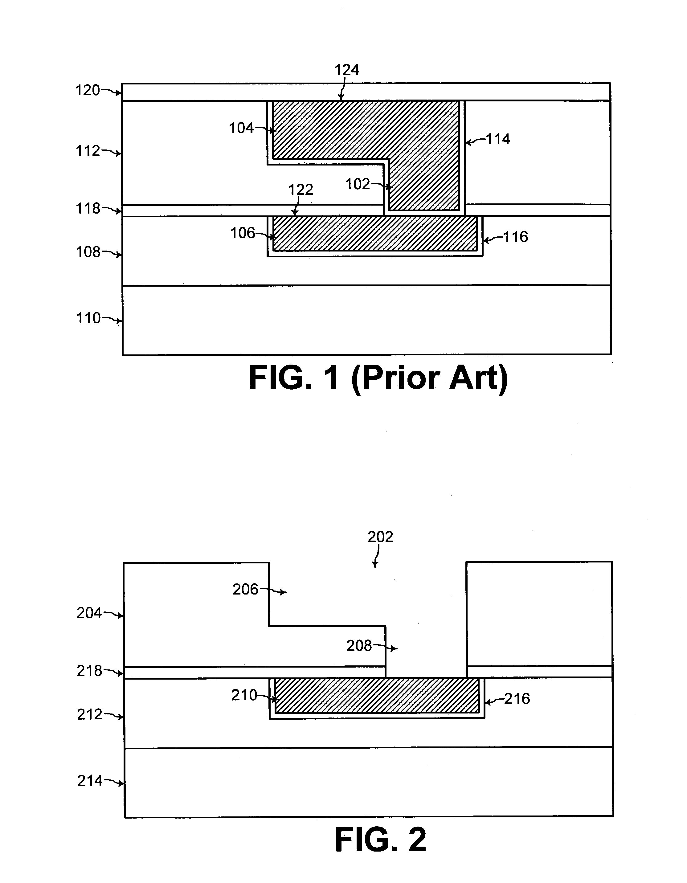
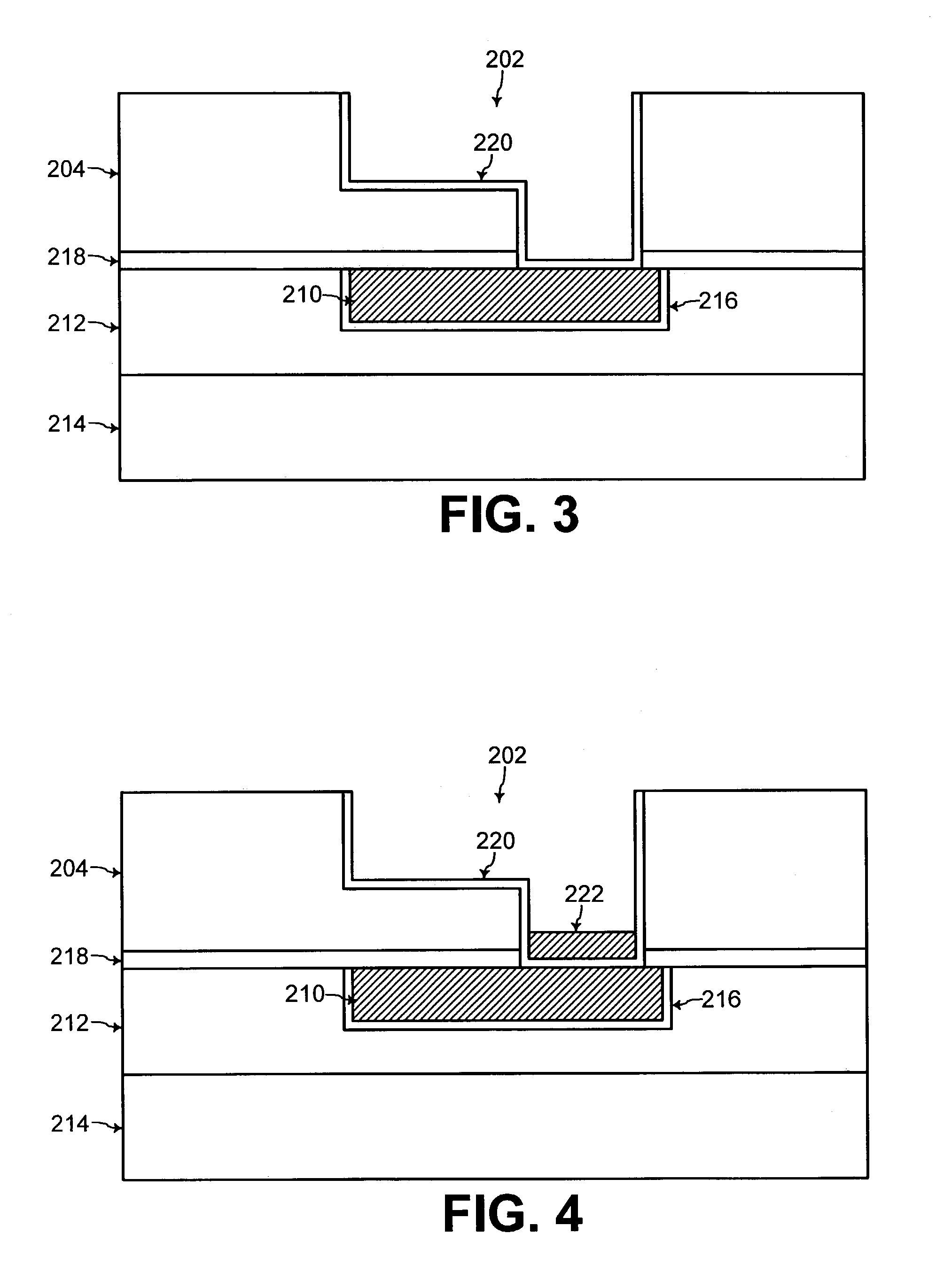
[0032]An embodiment of the present invention is described in reference to a dual damascene interconnect structure. However, aspects of the present invention may be used for forming any type of interconnect structure such as a via structure or a metal line structure formed individually, as would be apparent to one of ordinary skill in the art of integrated circuit fabrication from the description herein.

[0033]Referring to FIG. 2, a dual damascene opening 202 is formed within an upper dielectric layer 204. The dual damascene opening 202 includes an upper trench opening 206 and a lower via opening 208 formed on an underlying interconnect structure 210. The underlying interconnect structure 210 is formed within a lower dielectric layer 212 which is formed on a semiconductor substrate 214. In one embodiment of the present invention, the semiconductor substrate 214 is comprised of silicon, and the upper and lower dielectric layers 204 and 212 are comprised of silicon dioxide (SiO2) or a l...


PUM

PropertyMeasurementUnit
grain boundaryaaaaaaaaaa
conductiveaaaaaaaaaa
voltageaaaaaaaaaa

Abstract

An interconnect structure is formed with a plurality of layers of a conductive material with a grain boundary between any two adjacent layers of the conductive material. Such grain boundaries between layers of conductive material act as shunt by-pass paths for migration of atoms of the conductive material to minimize migration of atoms of the conductive material along the interface between a dielectric passivation or capping layer and the interconnect structure. When the interconnect structure is a via structure, each of the layers of the conductive material and each of the grain boundary are formed to be perpendicular to a direction of current flow through the via structure. Such grain boundaries formed between the plurality of layers of conductive material in the via structure minimize charge carrier wind-force along the direction of current flow through the via structure to further minimize electromigration failure of the via structure.

Description

TECHNICAL FIELD[0001]The present invention relates generally to interconnect technology in integrated circuit fabrication, and more particularly, to forming an interconnect structure with multiple layers of conductive material with a grain boundary formed between any two adjacent layers for minimizing electromigration failure of the interconnect structure.BACKGROUND OF THE INVENTION[0002]Common components of a monolithic IC (integrated circuit) include interconnect structures such as metal line structures and via structures for electrically connecting integrated circuit devices formed on a semiconductor substrate, as known to one of ordinary skill in the art of integrated circuit fabrication. A long-recognized important objective in the constant advancement of monolithic IC (Integrated Circuit) technology is the scaling-down of IC dimensions. Such scaling-down of IC dimensions reduces area capacitance and is critical to obtaining higher speed performance of integrated circuits. More...

Claims


Application Information

Patent Timeline
Patent Type & Authority Patents(United States)
IPC IPC(8): H01L21/44
CPCH01L21/76879H01L21/2885
Inventor TRAN, MINH QUOCYOU, LUWANG, FEIOKADA, LYNNE
Owner ADVANCED MICRO DEVICES INC
Why Eureka
Try Eureka