Protection of Cu damascene interconnects by formation of a self-aligned buffer layer

a buffer layer and damascene technology, applied in the field of electronic components, can solve the problems of damascene copper wiring patterns being exposed to air, damascene copper wiring patterns being difficult to pattern and use for metal wiring, and being subject to oxidation. , to achieve the effect of improving process yield and reliability, and high performan

Inactive Publication Date: 2011-10-04
NOVELLUS SYSTEMS
View PDF44 Cites 18 Cited by
  • Summary
  • Abstract
  • Description
  • Claims
  • Application Information

AI Technical Summary

Benefits of technology

[0011]Bearing in mind the problems and deficiencies of the prior art, it is therefore an object of the present invention to provide a method for fabricating high performance interconnection circuitry with improved process yield and reliability.
[0012]It is another object of the present invention to reduce defect sensitivity of copper interconnect metallurgy by improving its electromigration resistance.
[0013]A further object of the invention is to provide a method of forming a protective layer over a copper line that reduces electromigration failure of the interconnect line.
[0014]Still another object of the invention is to provide a method of forming and a protective cap or buffer layer over a copper line for improving the electromigration resistance of such interconnect line.
[0015]It is yet another object of the present invention to provide a method of buffering copper lines which does not affect the metal line integrity.

Problems solved by technology

However, copper is often difficult to pattern and use for metal wiring as it is easily oxidized when exposed to air.
Oxidation of copper interconnects undesirably increases the resistance of the wiring pattern.
However, the damascene copper wiring patterns may still be exposed to air, and thus, be subjected to oxidation.
With time and temperature, these oxides ultimately corrode the copper to result in formation of voids in the copper conductor, which are detrimental to the integrated circuit (IC) device and must be avoided.
However, it has been found that in copper damascene interconnection structures, the most likely point of failure during line current stress (electromigration) is this copper to dielectric barrier interface.
Whereas the electromigration resistance of copper is high enough to sustain the wear-out in normally designed conductor lines, defect-induced electromigration failures have been observed at the interface between the copper and dielectric barrier layer.
For instance, wherein copper oxides or hydroxides have been undesirably formed at such interfaces, voids will be formed in the copper layer, which hamper the electromigration characteristics of such copper interconnection.
Understandably, current density in these regions is considerably high during actual use, thereby causing early field fails due to defect sensitive electromigration failure.
Thus, despite repeated efforts, and various schemes in the prior art, manufacturing problems due to defect sensitive electromigration failure and corrosion remain.

Method used


Image

  • Protection of Cu damascene interconnects by formation of a self-aligned buffer layer
  • Protection of Cu damascene interconnects by formation of a self-aligned buffer layer
  • Protection of Cu damascene interconnects by formation of a self-aligned buffer layer

Examples


example

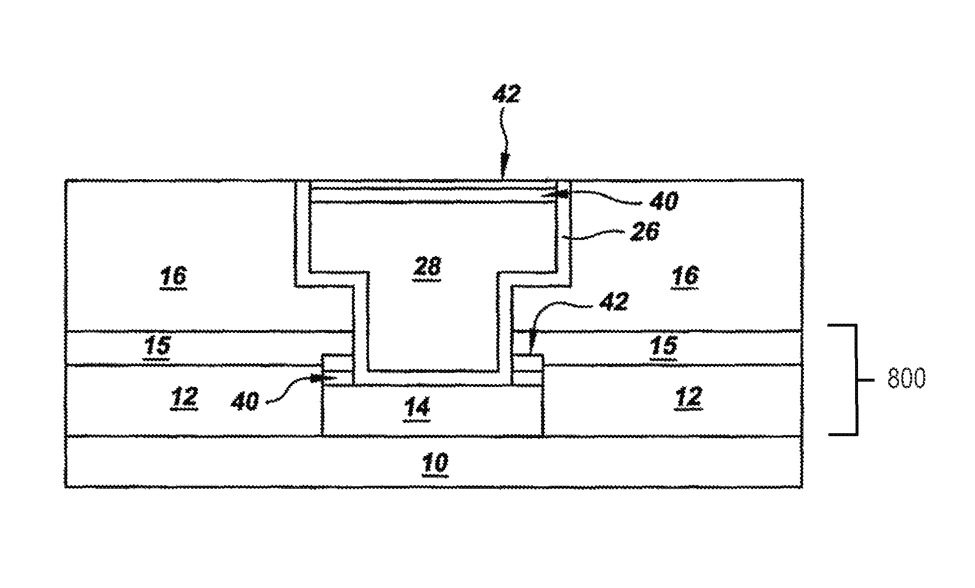
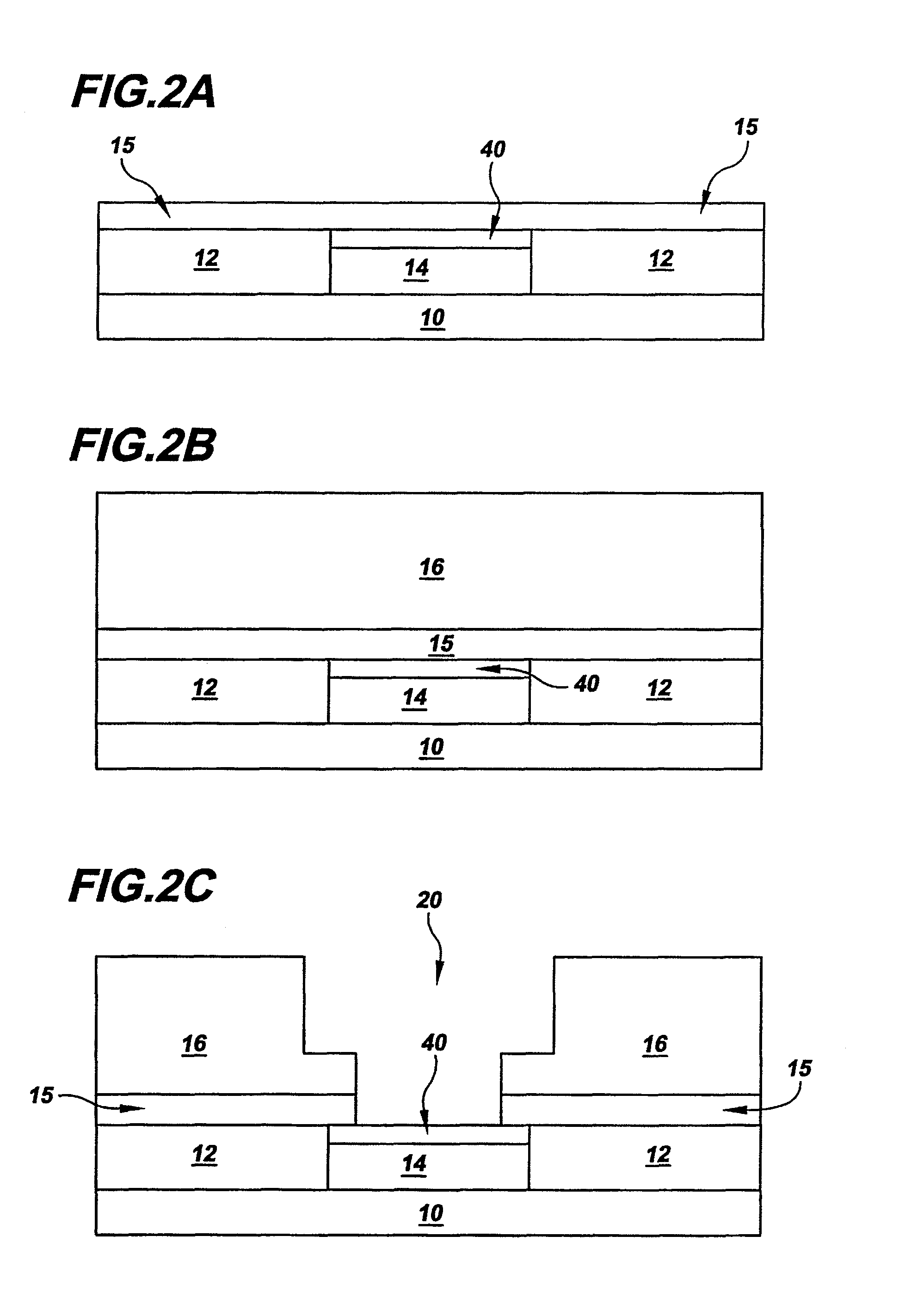
[0062]Formation of a CuSix / SiN protective self-aligned buffer layer 40 / dielectric cap layer 42 may be accomplished using the following steps:

Station 1: Providing a structure 100 having exposed copper layer 14 into a first chamber of a multichamber processing tool, wherein such structure is cleaned followed by heating the structure to a temperature ranging from about 20° C. to about 500° C.

[0063]Station 2: The cleaned, preheated structure is then moved into a second chamber under a continuous vacuum, wherein SiH4 is flown into such chamber at a rate ranging from about 1 sccm to about 100 sccm, under temperatures ranging from about 150° C. to about 250° C., and pressures range of about 10 mTorr to about 100 Torr. SiH4 molecules react with copper atoms at a top portion of the copper layer 14 to transform such top copper layer portion to a CuSix protective self-aligned buffer layer 40 within the copper layer 14. This process forms CuSix, while avoiding Si diffusion, with insignificant r...


PUM

PropertyMeasurementUnit
temperatureaaaaaaaaaa
pressuresaaaaaaaaaa
temperaturesaaaaaaaaaa

Abstract

Methods of protecting exposed metal damascene interconnect surfaces in a process for making electronic components and the electronic components made according to such methods. An integrated circuit structure having damascene regions with exposed metal surfaces is provided into a closed processing chamber, whereby a first reactant is contacted to the exposed metal surfaces to transform a top portion of the metal layer into a protective self-aligned buffer layer. Reacting molecules of the first reactant with metal atoms of this metal layer forms the protective self-aligned buffer layer entirely within such metal layer. Alternatively, adsorbing surface-active reactant molecules onto the exposed metal surface forms the protective self-aligned buffer layer. A second reactant may be contacted to the protective self-aligned buffer layer to form a self-aligned dielectric cap layer directly over the protective self-aligned buffer layer.

Description

BACKGROUND OF THE INVENTION[0001]1. Field of the Invention[0002]This invention relates to the making of electronic components such as integrated circuit semiconductor devices having electrical interconnection structures within the component and, more particularly, to a self-aligned protective buffer layer over copper damascene interconnects.[0003]2. Description of Related Art[0004]In semiconductor fabrication processes, layers of insulating, conducting and semiconducting materials are commonly deposited and patterned to form integrated circuits (IC). Contact vias, i.e., openings, are also commonly formed in insulating materials known as interlevel dielectrics (ILDs). These vias are filled with conductive material to interconnect electrical devices and wiring at various levels.[0005]Damascene and dual damascene processing similarly involve etching openings to define wiring patterns and contacts in multiple layers of insulating dielectric layers for electrically connecting metallizati...

Claims


Application Information

Patent Timeline
Patent Type & Authority Patents(United States)
IPC IPC(8): H01L23/48
CPCH01L21/76834H01L21/76846H01L21/76849H01L21/76856H01L21/76867H01L21/76886H01L21/76831
Inventor VAN SCHRAVENDIJK, BARTMOUNTSIER, THOMAS WSANGANERIA, MAHESH KALERS, GLENN BSHAVIV, ROEY
Owner NOVELLUS SYSTEMS
Why Eureka
Try Eureka