Semiconductor Light-Emitting Element, Manufacturing Method and Mounting Method of the Same and Light-Emitting Device

a technology of semiconductors and light-emitting elements, which is applied in the manufacturing of semiconductor/solid-state devices, semiconductor devices, electrical devices, etc., can solve the problems of high possibility of junction yield reduction, high cost, and high cost, and achieve low cost and high productivity. , the effect of low cos

Active Publication Date: 2007-11-15
EVERLIGHT ELECTRONICS
View PDF0 Cites 112 Cited by
  • Summary
  • Abstract
  • Description
  • Claims
  • Application Information

AI Technical Summary

Benefits of technology

[0062] In accordance with the semiconductor light-emitting element of the present invention and the manufacturing method and mounting method of the same, since the area on the second n-electrode to be joined to the electrode of a circuit board is made larger than the first n-electrode with the area on the second p-electrode being made smaller than that of the first p-electrode, it becomes possible to carry out a mounting process on a circuit board at low costs by using a conductive bonding material such as solder.
[0063] Moreover, in accordance with the light-emitting device of the present invention, since the semiconductor light-emitting element can be mounted on a circuit board at low costs by using a conductive bonding material such as solder, it is possible to achieve high productivity, high junction quality and high yield.

Problems solved by technology

To form a number of bumps on the p-electrode is not desirable because of a higher possibility of a reduction in the yield of junctions and of short-circuiting and connection failure, due to positional deviations at the time of mounting.

Method used


Image

  • Semiconductor Light-Emitting Element, Manufacturing Method and Mounting Method of the Same and Light-Emitting Device
  • Semiconductor Light-Emitting Element, Manufacturing Method and Mounting Method of the Same and Light-Emitting Device
  • Semiconductor Light-Emitting Element, Manufacturing Method and Mounting Method of the Same and Light-Emitting Device

Examples


first embodiment

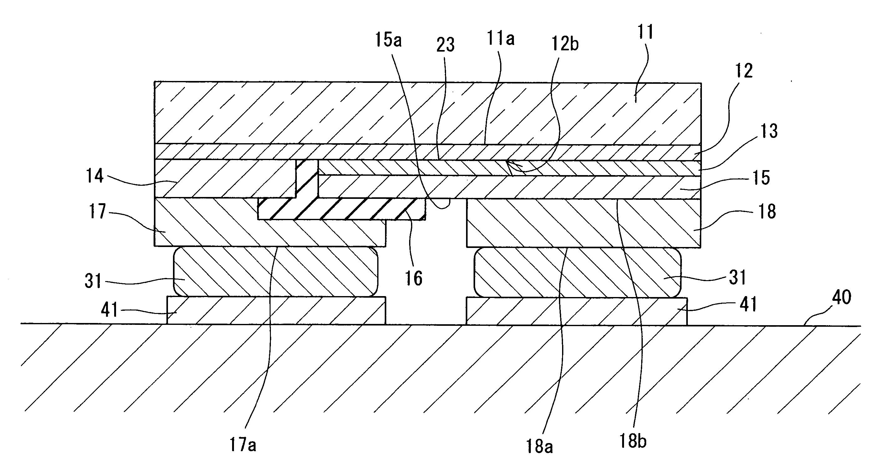
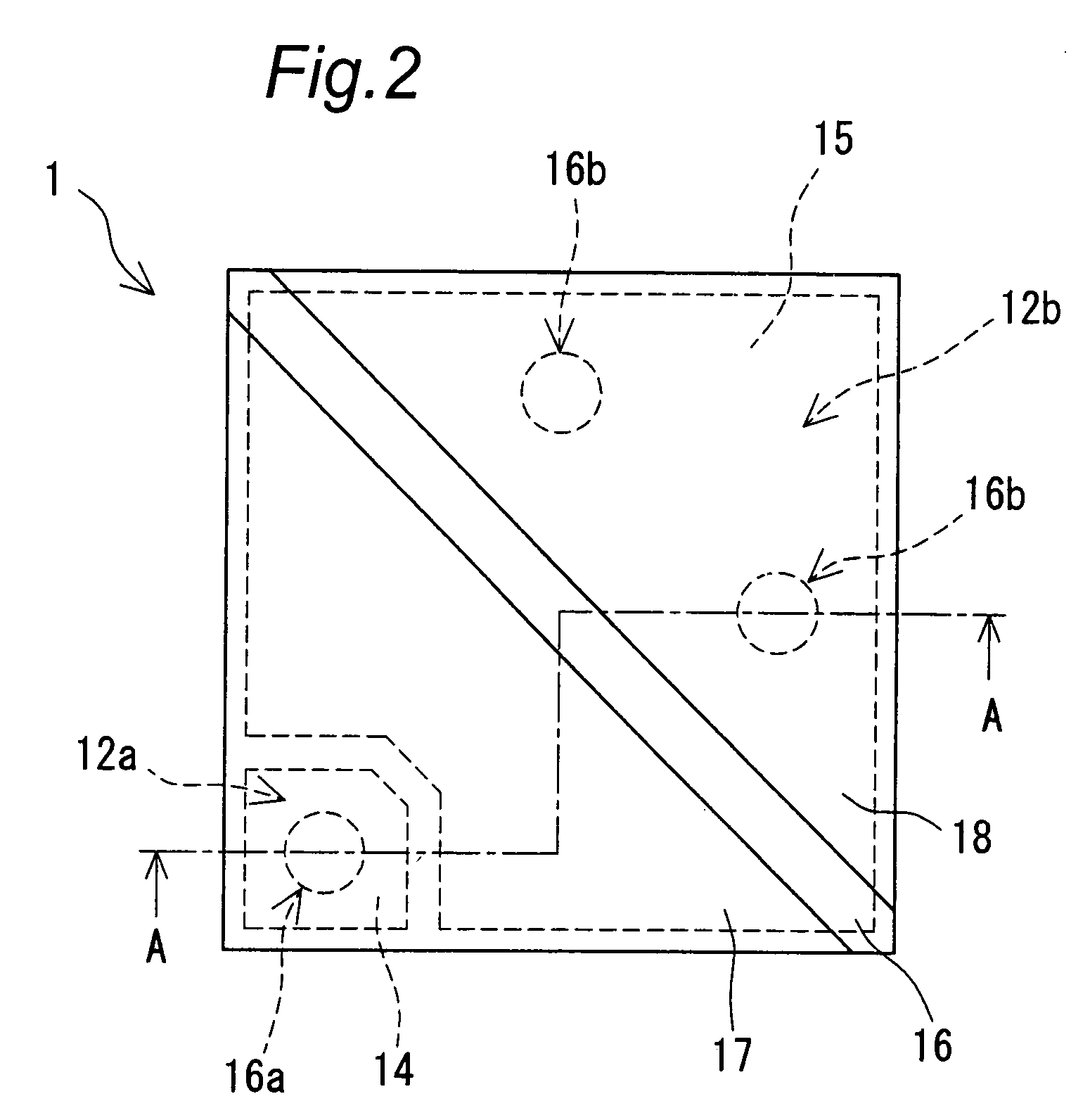
[0084]FIG. 1 is a longitudinal cross-sectional view that shows a light-emitting device in which an LED chip 1, which is one example of a semiconductor light-emitting element in accordance with a first embodiment of the present invention, is mounted on a circuit board 40 through solder 31, which is one example of a conductive bonding material layer, and FIG. 2 is a bottom view of the LED chip 1. FIG. 1 schematically shows a cross section taken along line A-A in FIG. 2. Here, in the cross-sectional view of FIG. 1, for convenience of explanation, one portion thereof is indicated in an exaggerated manner. The following explanation will be given so as to laminate respective layers and respective electrodes downward in the Figure.

[0085] In FIG. 1, the LED chip 1 is provided with a bare chip 10 (see FIG. 3) including an element substrate 11, an n-type semiconductor layer 12 formed on the element substrate 11 so as to cover the element substrate 11, a p-type semiconductor layer 13 formed o...

second embodiment

[0107]FIG. 9 is a longitudinal cross-sectional view that shows a light-emitting device in which an LED chip 1a in accordance with a second embodiment of the present invention, is mounted on a circuit board 40 through solder 31, which is one example of a conductive bonding material layer. FIG. 10 is a bottom view of the LED chip 1a, and FIG. 11 is a bottom view in a state before the formation of the second n-electrode 17 and the second p-electrode 18 of the LED chip 1a. FIG. 9 is a drawing that schematically shows a cross section at a position of line B-B in FIG. 10 and FIG. 11. Here, in the cross-sectional view of FIG. 9, for convenience of explanation, one portion thereof is indicated in an exaggerated manner. Moreover, a portion with slanting lines in FIG. 11 is not given to indicate cross-sectional lines, but given to help understanding of the areas of the conductive layer 14 (portion with thin slanting lines) and a second insulating layer (portion with thick slanting lines).

[01...


PUM


Abstract

An LED chip of the present invention has a structure in which an n-type semiconductor layer and a p-type semiconductor layer are successively formed on the lower face of an element substrate, with the p-type semiconductor layer being formed on an area except for an area for an n-electrode. A first n-electrode is formed on the area for the n-electrode and a first p-electrode is formed on the p-type semiconductor layer. A first insulating layer having openings and is formed on the first n-electrode and the first p-electrode, and a second n-electrode and a second p-electrode having virtually the same size are formed on the first insulating layer. With this arrangement, the electrode on the n-type semiconductor layer can be made larger, thereby a mounting process of LED chips onto a circuit board can be executed by using solder at low costs.

Description

TECHNICAL FIELD [0001] The present invention relates to a semiconductor light-emitting element, a manufacturing method and a mounting method of the same and a light-emitting device formed by mounting such semiconductor light-emitting elements on a circuit board. BACKGROUND ART [0002] In recent years, a technique in which a number of bare chips of semiconductor light-emitting elements are mounted on a circuit board, typically represented by a light emitting diode (hereinafter, referred to as “LED”), to manufacture illuminating and display devices or the like has been widely utilized. With respect to the mounting technique for mounting the bare chips for the LED (hereinafter, referred to as “LED chip”) on a circuit board, a flip chip junction utilizing bumps, for example, described in Patent Document 1 and Patent Document 2, has been generally used. [0003]FIG. 16 is a cross-sectional view that schematically shows a state in which LED chips having a typically conventional structure are...

Claims


Application Information

Patent Timeline
Patent Type & Authority Applications(United States)
IPC IPC(8): H01L33/00H01L33/26H01L33/38H01L33/58H01L33/60H01L33/62
CPCH01L33/38H01L33/387H01L33/44H01L33/62H01L2924/12041H01L2924/01004H01L2924/01078H01L2924/01079H01L2933/0016H01L2224/16H01L24/05H01L24/06H01L24/13H01L24/16H01L2224/05568H01L2224/05573H01L2224/0603H01L2224/06051
Inventor HIGASHI, KAZUSHIISHITANI, SHINJI
Owner EVERLIGHT ELECTRONICS
Why Eureka
Try Eureka