Method for forming a semiconductor on insulator structure

a technology of insulator structure and semiconductor, which is applied in the direction of semiconductor devices, instruments, electrical devices, etc., can solve the problems of significant wafer waste, difficult to achieve uniform polished surface, and non-uniform thickness and surface texture of wafers

Inactive Publication Date: 2007-11-15
CORNING INC
View PDF35 Cites 4 Cited by
  • Summary
  • Abstract
  • Description
  • Claims
  • Application Information

AI Technical Summary

Benefits of technology

[0024] The invention will be understood more easily and other objects, characteristics, details and advantages thereof will become more clearly apparent in the course of the following explanatory description, which is given, without in any way implying a limitation, with reference to the attached Figures. It is intended that all such additional systems, methods features and advantages be included within this description, be within the scope of the present invention, and be protected by the accompanying claims.

Problems solved by technology

Semiconductor devices are usually square or rectangular, yet they are always manufactured on round wafers, resulting in significant wafer waste.
But even if rectangular semiconductor wafers were available, uniformity of the polished surface would be difficult to achieve.
If a rectangular wafer is polished, the pressure and time in contact with the polishing pad across the whole surface is more variable than with a round wafer, especially at the corners, where the wafer tends to be preferentially machined, resulting in wafer thickness and surface texture non-uniformity.

Method used


Image

  • Method for forming a semiconductor on insulator structure
  • Method for forming a semiconductor on insulator structure
  • Method for forming a semiconductor on insulator structure

Examples


Embodiment Construction

[0029] In the following detailed description, for purposes of explanation and not limitation, example embodiments disclosing specific details are set forth to provide a thorough understanding of the present invention. However, it will be apparent to one having ordinary skill in the art, having had the benefit of the present disclosure, that the present invention may be practiced in other embodiments that depart from the specific details disclosed herein. Moreover, descriptions of well-known devices, methods and materials may be omitted so as not to obscure the description of the present invention. Finally, wherever applicable, like reference numerals refer to like elements.

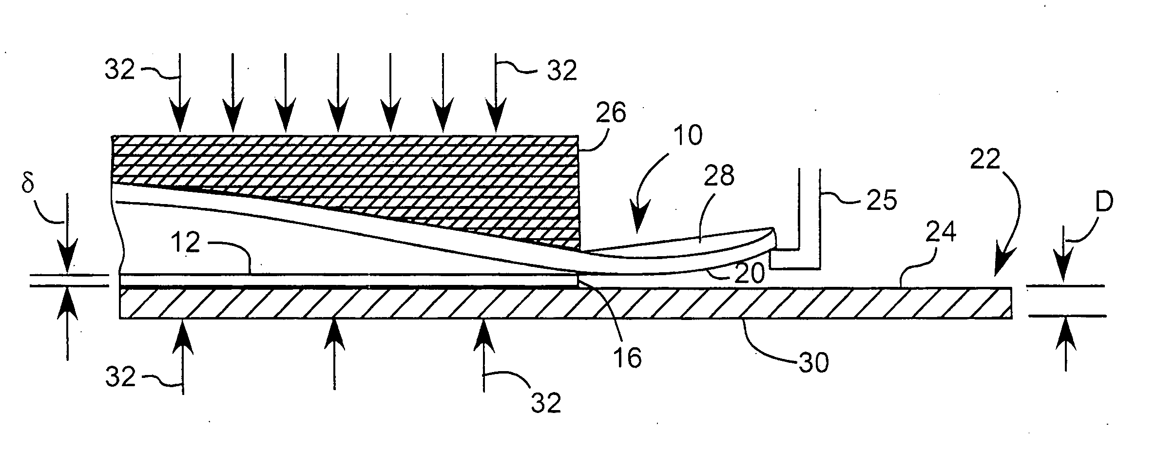
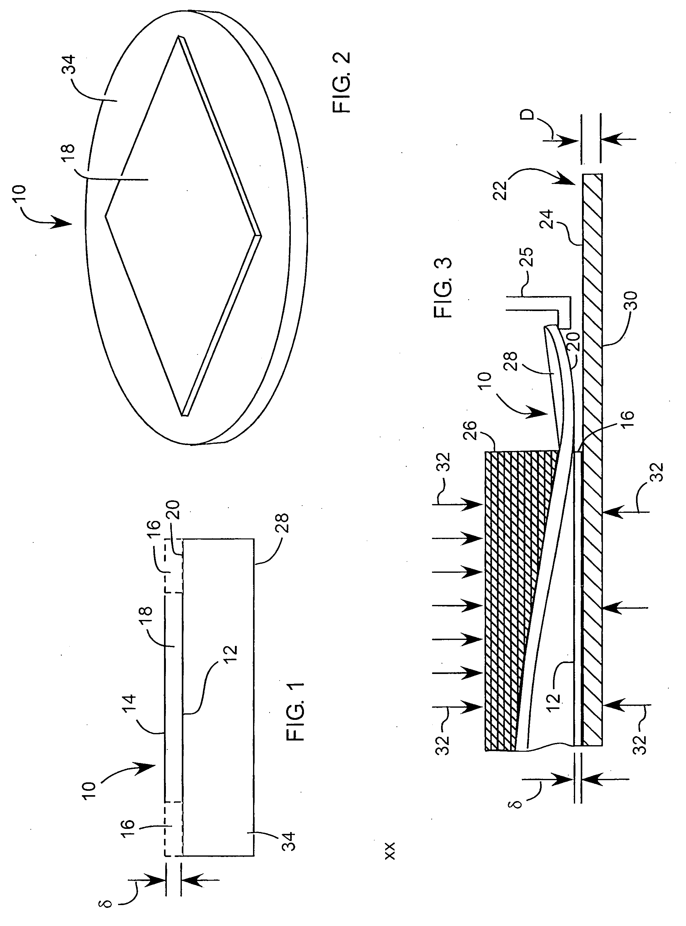
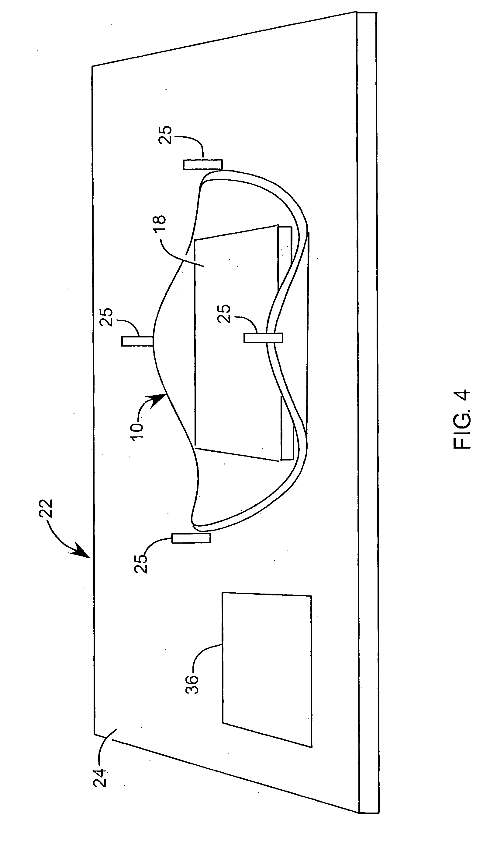
[0030] In accordance with an embodiment of the present invention, a method of transferring a rectangular shaped wafer of semiconductor material from a round precursor wafer is disclosed. Referring to FIGS. 1-2, a round semiconductor wafer 10 having substantially planar and parallel first and second surfaces is io...


PUM


Abstract

A method of bonding a thin semiconductor film onto a rectangular substrate is disclosed. The method makes it possible to exfoliate rectangular semiconductor films from a round precursor semiconductor wafer, thereby providing for efficient tiling of the substrate with semiconductor film. The method includes the steps of creating a damage zone in the precursor wafer by ion implantation of the wafer, removing a portion of the wafer to formed a raised portion, bonding the raised portion of the wafer to the substrate, and exfoliating the bonded raised portion.

Description

BACKGROUND OF THE INVENTION [0001] 1. Field of the Invention [0002] This invention is directed to a method of forming a semiconductor-on-insulator structure, and in particular, a silicon-on-glass structure. [0003] 2. Technical Background [0004] The economic manufacture of silicon wafers used for the production of semiconductor devices is well known. All such wafers are thin round discs, and semiconductor manufacturing systems have been optimized for the production of thin round discs. The current standard size for silicon wafers is approximately 300 mm in diameter. [0005] Flat display glass panels, such as those used in the manufacture of liquid crystal displays for example, require thin films of silicon to be deposited upon them in order to produce the semiconductor pixel switches. One method of performing this deposition is by transferring exfoliated, thin films from a prime silicon wafer onto the display glass. [0006] Prior to exfoliation, the wafers are ion implanted to produce ...

Claims


Application Information

Patent Timeline
Patent Type & Authority Applications(United States)
IPC IPC(8): H01L21/46H01L29/06
CPCH01L21/76254H01L24/26H01L2924/10253H01L2924/01075H01L2924/01023H01L2224/83894H01L2924/01004H01L2924/01033H01L2924/01058H01L2924/01077H01L2924/01082H01L2924/09701H01L2924/30105H01L2924/01005H01L2924/01006H01L2924/01019H01L2924/3512H01L2924/00H01L2924/15787H01L2924/15788G02F1/1333H01L21/762
Inventor STOCKER, MARK ANDREW
Owner CORNING INC
Why Eureka
Try Eureka