Multilayer winding inductor

a multi-layer winding and inductor technology, applied in the direction of transformers/inductance coils/windings/connections, continuous variable inductances/transformers, inductances, etc., can solve the problem of difficult to increase integration and reduce manufacturing costs, and the size dsub>1 /sub> of the planar spiral inductor is difficult to redu

Active Publication Date: 2007-11-22
VIA TECH INC
View PDF3 Cites 87 Cited by
  • Summary
  • Abstract
  • Description
  • Claims
  • Application Information

AI Technical Summary

Problems solved by technology

Thus, it is difficult to decrease the size d1 of the planar spiral inductor.
That is, the planar spiral inducto...

Method used


Image

  • Multilayer winding inductor
  • Multilayer winding inductor
  • Multilayer winding inductor

Examples


Embodiment Construction

[0023]The following description is of the best-contemplated mode of carrying out the invention. This description is provided for the purpose of illustrating the general principles of the invention and should not be taken in a limiting sense. The scope of the invention is best determined by reference to the appended claims. The multilayer winding inductor of the invention will be described in the following with reference to the accompanying drawings.

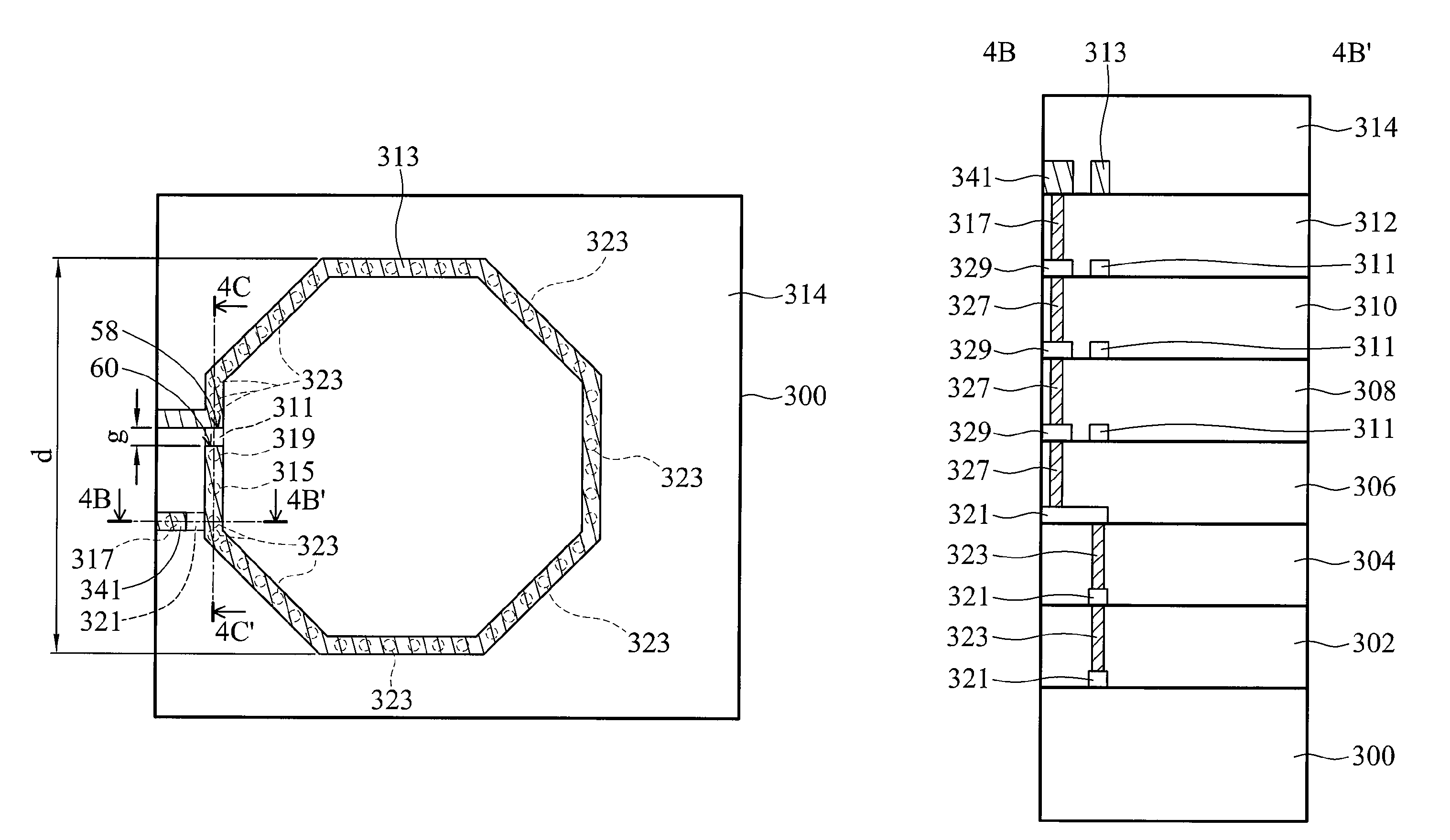
[0024]FIG. 3A is a plan view of an embodiment of a multilayer winding inductor. FIGS. 3B and 3C are cross-sections along 3B-3B′ and 3C-3C′ lines, respectively. The multilayer winding inductor comprises multi-level and single-level interconnect structures embedded in an insulating layer on a substrate 300. The substrate 300 may be a silicon substrate or other semiconductor substrate. The substrate may include various elements, such as transistors, resistors or other well known semiconductor elements. Moreover, the substrate 300 may also in...


PUM


Abstract

A multilayer winding inductor. The inductor at least includes multi-level interconnect and single-level interconnect structures. The multi-level interconnect structure includes a plurality of conductive plugs and a plurality of looped conductive traces overlapping and separated from each other. Each looped conductive trace has a gap to define first and second ends and at least two conductive plugs disposed between the neighboring looped conductive traces. The single-level interconnect structure is located over the multi-level interconnect structure, comprising an uppermost looped conductive trace and a second conductive plug. The uppermost looped conductive trace has a gap to define first and second ends, and the second conductive plug is disposed between the second end of the uppermost looped conductive trace and the first end of the looped conductive trace adjacent thereto, thereby electrically connecting the multi-level and single-level interconnect structures.

Description

BACKGROUND OF THE INVENTION[0001]1. Field of the Invention[0002]The invention relates to a semiconductor device, and in particular to an on-chip inductor with a multi-level interconnect structure.[0003]2. Description of the Related Art[0004]Many digital and analog elements and circuits have been successfully applied in semiconductor integrated circuits. Such elements may include passive components, such as resistors, capacitors, or inductors. Typically, a semiconductor integrated circuit is formed on a silicon substrate. One or more dielectric layers are disposed on the substrate and one or more conductive layers are disposed in the dielectric layers. Those conductive layers may be employed to form on-chip elements, such as on-chip inductors, by current semiconductor technologies.[0005]Conventionally, the on-chip inductor is formed over a semiconductor substrate and employed in integrated circuits designed for radio frequency (RF) band. FIGS. 1A and 1B illustrate a plan view of a co...

Claims


Application Information

Patent Timeline
IPC IPC(8): H01L29/00
CPCH01F17/0013H01F2017/002H01L23/5227H01L28/10H01L2924/0002H01L2924/00
Inventor LEE, SHENG-YUAN
Owner VIA TECH INC
Why Eureka
Try Eureka