Nitride based light emitting device

a light emitting device and nitride technology, applied in the direction of semiconductor devices, basic electric elements, electrical apparatus, etc., can solve the problems of many defects having a serious effect on the performance of the resulting led, the difficulty of growth of the based semiconductor, and the failure to meet the requirements of high-quality substrates, etc., to achieve efficient confinement of electrons and improve the reliability of the light emitting device

Active Publication Date: 2007-11-29
LG ELECTRONICS INC +1
View PDF7 Cites 43 Cited by
  • Summary
  • Abstract
  • Description
  • Claims
  • Application Information

AI Technical Summary

Benefits of technology

[0021]An object of the present invention is to provide a nitride based light emitting device which can adjust or restrict generation of strain and imperfections in solids, and achieve efficient confinement of electrons and holes within an active layer, resulting in an improvement in the reliability of the light emitting device.

Problems solved by technology

Meanwhile, one of the reasons why the GaN-based semiconductors have a difficulty in growth as compared to other III-V compound semiconductors is that there are no high quality substrates, namely, wafers made of GaN, InN, AlN, or the like.
This may cause many defects having a serious effect on the performance of the resulting LED.
Moreover, the strain is locally generated, and thus, may hinder efficient electron-hole coupling required for emitting light.
However, the partially inserted InGaN layer may restrict efficient confinement of electrons and holes within an active layer, thus causing a degradation in optical efficiency.

Method used


Image

  • Nitride based light emitting device
  • Nitride based light emitting device
  • Nitride based light emitting device

Examples


first embodiment

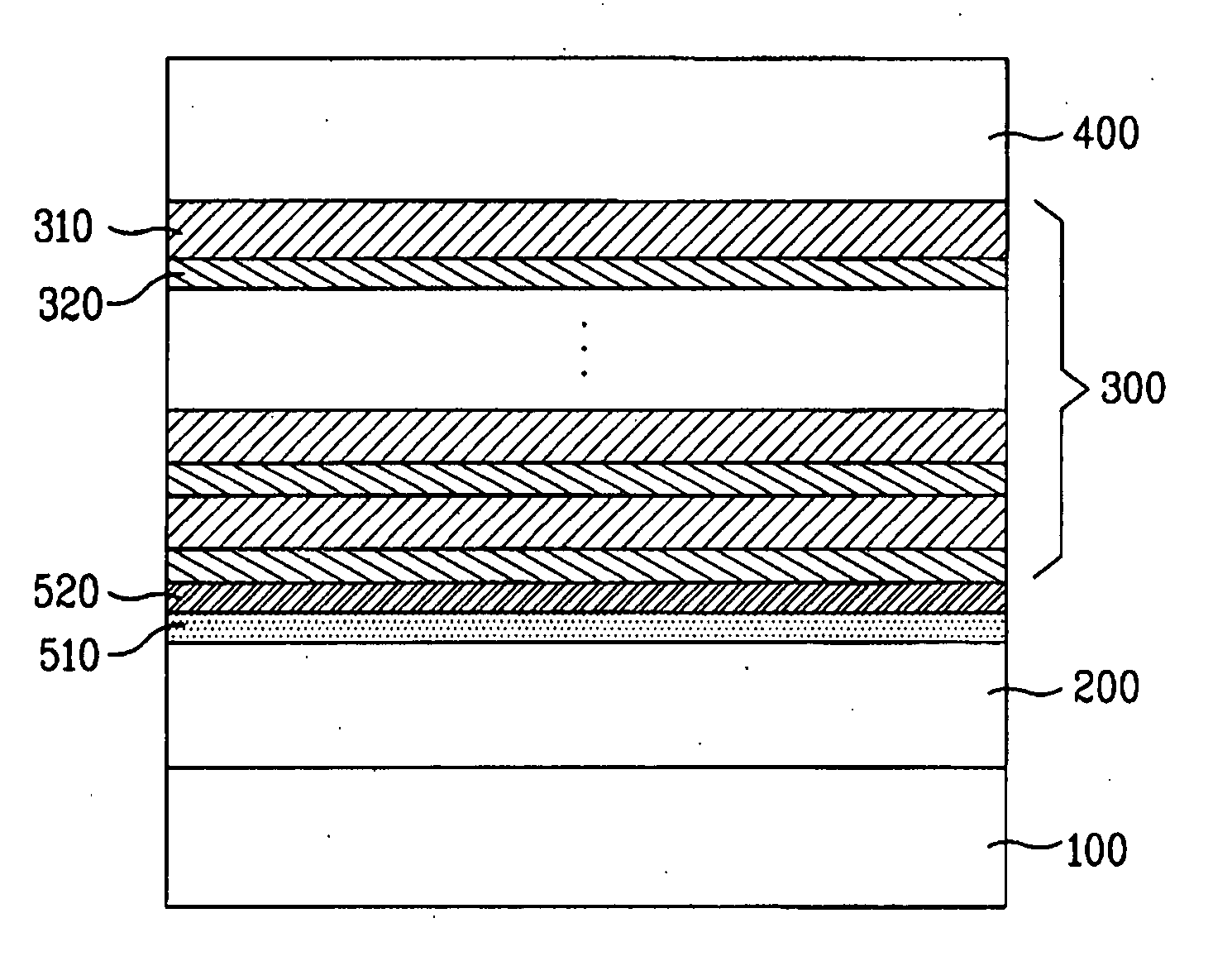
[0087]As described above with reference to FIG. 3, the n-type GaN semiconductor layer 200 is formed over the substrate 100. The active layer 300, which is made of GaInN, is formed over the n-type GaN semiconductor layer 200, and in turn, the p-type GaN semiconductor layer 400 is formed over the active layer 300.

[0088]In this case, the In composition within the well layer 320 of the active layer 300 may be larger than the In composition of the barrier layer 310.

[0089]FIG. 4 is an energy band diagram of the structure shown in FIG. 3. The first insertion layer 510, which is made of GaInN, is located at a boundary between the active layer 300 of the quantum well structure and the n-type semiconductor layer 200, and the second insertion layer 520 is located adjacent to the first insertion layer 510.

[0090]More specifically, the first insertion layer 510 is located between the n-type GaN semiconductor layer 200 and the first well layer 320 of the active layer 300. The In composition of GaI...

second embodiment

[0092]As shown in FIG. 6, the n-type GaN semiconductor layer 200 is formed over the substrate 100, and the active layer 300 is formed over the n-type GaN semiconductor layer 200. In turn, the p-type GaN semiconductor layer 400 is formed over the active layer 300.

[0093]In this case, the first insertion layer 510, which is made of GaInN, and the second insertion layer 510, which is made of AlGaInN, are formed between the n-type semiconductor layer 200 and the active layer 300. Specifically, there are provided a plurality of first insertion layers 510 and a plurality of second insertion layers 520, which are arranged alternately. That is to say, each first insertion layer 510 may pair with the corresponding second insertion layer 520.

[0094]FIG. 7 is an energy band diagram of the above described structure according to the present embodiment. As shown, both the barrier layer 310 and the well layer 320 of the active layer 300 are made of GaInN, and the first insertion layer 510 has a band...

third embodiment

[0099]As shown in FIG. 8, the insertion layers 510 and 520, made of GaInN / AlGaInN, may be formed between the active layer 300 and the p-type GaN semiconductor layer 400.

[0100]The insertion layers 510 and 520 may be located between the active layer 300 and the p-type GaN semiconductor layer 400. Similar to the above mentioned insertion layers between the n-type GaN semiconductor layer 200 and the active layer 300, the insertion layers 510 and 520 can relieve strain, and achieve an improvement in the supply of electric current and the confinement of carriers.

[0101]FIG. 9 is an energy band diagram of the above described structure. As shown, the first insertion layer 510 may be located adjacent to the active layer 300, and the second insertion layer 520 may be located at the outside of the first insertion layer 510. Alternatively, the second insertion layer 520 may be located adjacent to the active layer 300, and the first insertion layer 510 may be located at the outside of the second ...


PUM


Abstract

A nitride based light emitting device is disclosed. More particularly, a nitride based light emitting device capable of improving light emitting efficiency and reliability thereof is disclosed. The nitride based light emitting device includes a first conductive semiconductor layer connected to a first electrode, a second conductive semiconductor layer connected to a second electrode, an active layer located between the first conductive semiconductor layer and the second conductive semiconductor layer and having a quantum well structure, a first insertion layer located in at least one of a boundary between the first conductive semiconductor layer and the active layer and a boundary between the second conductive semiconductor layer and the active layer, and a second insertion layer located adjacent to the first insertion.

Description

[0001]This application claims the benefit of the Korean Patent Application No. 10-2006-0046081, filed on, May 23, 2006, which is hereby incorporated by reference as if fully set forth herein.BACKGROUND OF THE INVENTION[0002]1. Field of the Invention[0003]The present invention relates to a nitride based light emitting device, and more particularly, to a nitride based light emitting device which can achieve an improvement in light emitting efficiency and reliability.[0004]2. Discussion of the Related Art[0005]Light emitting diodes (LEDs) are well known as a semiconductor light emitting device which converts current to light, to emit light. Since a red LED using GaAsP compound semiconductor was commercially available in 1962, it has been used, together with a GaP:N-based green LED, as a light source in electronic apparatuses including telecommunication apparatuses, for image display.[0006]The wavelength of light emitted from such an LED depends on the semiconductor material used to fab...

Claims


Application Information

Patent Timeline
Patent Type & Authority Applications(United States)
IPC IPC(8): H01L33/00H01L29/225H01L29/24H01L33/06H01L33/32
CPCH01L33/32H01L33/06
Inventor SHIN, JOHNG EON
Owner LG ELECTRONICS INC
Why Eureka
Try Eureka