Semiconductor Device and Method for Manufacturing the Same

Active Publication Date: 2007-11-29
HAMAMATSU PHOTONICS KK
View PDF14 Cites 7 Cited by
  • Summary
  • Abstract
  • Description
  • Claims
  • Application Information

AI Technical Summary

Benefits of technology

[0013] In this case, the semiconductor device with the above-mentioned functions can be manufactured readily by adhering on the resin sheet.
[0014] By this invention, a semiconductor device can be realized with which the distortion and c

Problems solved by technology

In this case, the thinned portion may become distorted due to expansion or contraction of the

Method used


Image

  • Semiconductor Device and Method for Manufacturing the Same
  • Semiconductor Device and Method for Manufacturing the Same
  • Semiconductor Device and Method for Manufacturing the Same

Examples


Example

EXPLANATION OF REFERENCE NUMERALS

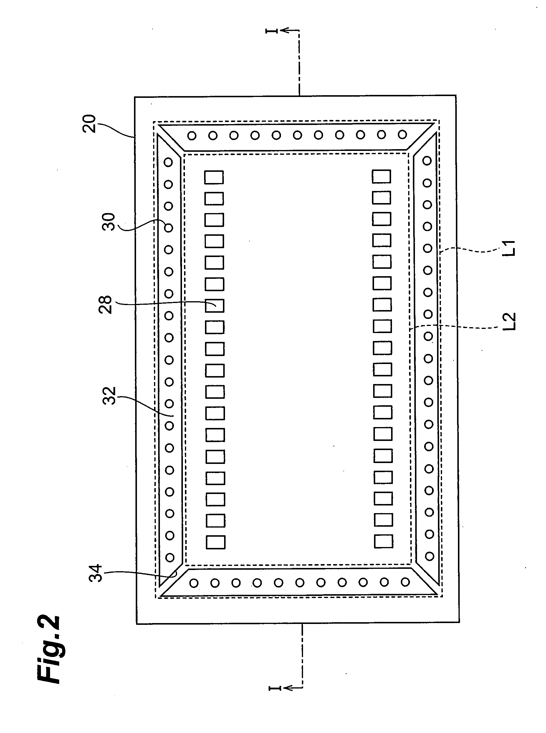
[0022]1 . . . semiconductor device [0023]10 . . . semiconductor substrate [0024]14 . . . thinned portion [0025]15 . . . outer edge [0026]16 . . . electrode [0027]18 . . . accumulation layer [0028]20 . . . wiring substrate [0029]22 . . . electrode [0030]24 . . . lead terminal [0031]28 . . . chip resistor [0032]30 . . . conductive bumps [0033]32 . . . resin [0034]34 . . . communicating portion

BEST MODES FOR CARRYING OUT THE INVENTION

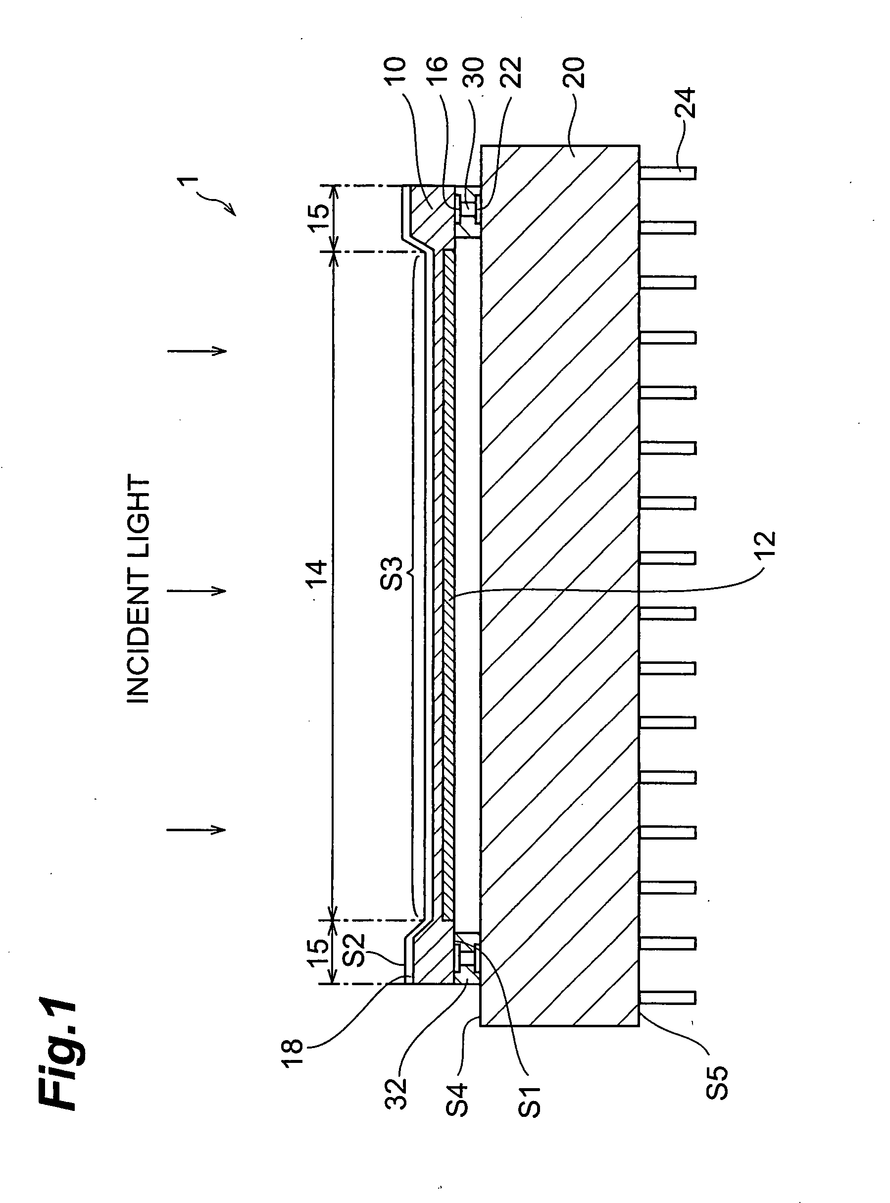
[0035] Preferred embodiments of this invention's semiconductor device shall now be described in detail along with the drawings. In the description of the drawings, the same elements shall be provided with the same symbols and overlapping description shall be omitted. The dimensional proportions in the drawings do not necessary match those of the description.

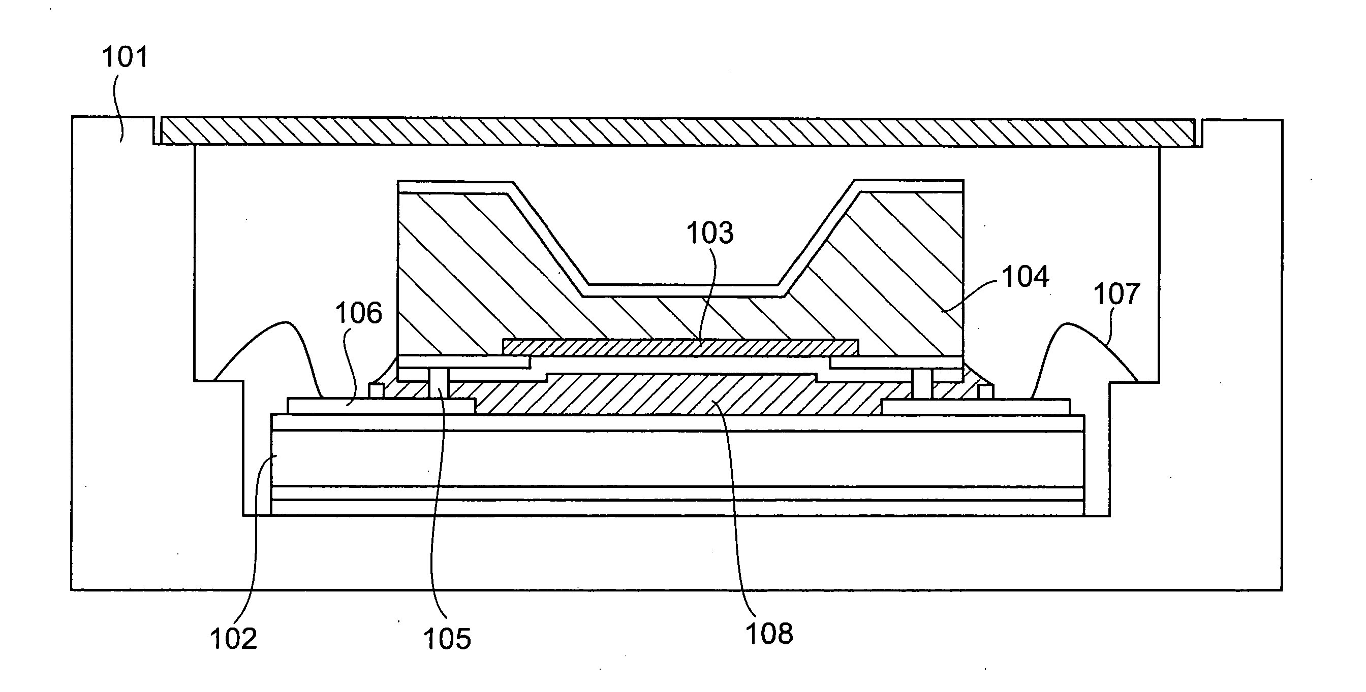
[0036]FIG. 1 is a sectional view of an embodiment of this invention's semiconductor device. A semiconductor device 1 has a semiconductor substrate 10, a wiring subst...


PUM


Abstract

With this semiconductor device, the distortion and cracking of a thinned portion of a semiconductor substrate are prevented to enable high precision focusing with respect to a photodetecting unit and uniformity and stability of high sensitivity of the photodetecting unit to be maintained. A semiconductor device 1 has a semiconductor substrate 10, a wiring substrate 20, conductive bumps 30, and a resin 32. A CCD 12 and a thinned portion 14 are formed on semiconductor substrate 10. Electrodes 16 of semiconductor substrate 10 are connected via conductive bumps 30 to electrodes 22 of wiring substrate 20. Insulating resin 32 fills a gap between outer edge 15 of thinned portion 14 and wiring substrate 20 to reinforce the bonding strengths of conductive bumps 30. This resin 32 is a resin sheet that has been formed in advance so as to surround a periphery of a gap between thinned portion 14 and wiring substrate 20 except for portions of the periphery.

Description

TECHNICAL FIELD [0001] This invention concerns a semiconductor device and a method for manufacturing the same, and particularly concerns a back-illuminated semiconductor device and a method for manufacturing the same. BACKGROUND ART [0002] A so-called back-illuminated semiconductor photodetecting device has been known conventionally as a semiconductor device. This type of semiconductor device has a semiconductor substrate and has a photodetecting unit on one surface of the semiconductor substrate. A portion of the semiconductor substrate on the side opposite the photodetecting unit is trimmed to form a recessed portion in the semiconductor substrate. A thinned portion is thus provided at the portion of the semiconductor substrate at which the photodetecting unit is disposed. This thinned portion is provided to accommodate ultraviolet rays, soft X-rays, electronic beams, and other energy rays that will be absorbed and cannot be detected at high sensitivity by a thick semiconductor su...

Claims


Application Information

Patent Timeline
IPC IPC(8): H01L31/02H01L31/18H01L27/14H01L21/56H01L21/60H01L27/148H04N5/335H04N5/365H04N5/369H04N5/372
CPCH01L21/563H01L27/1464H01L24/90H01L27/14636H01L27/14806H01L2224/73203H01L2224/81203H01L2224/81801H01L2224/83191H01L2224/83194H01L2924/01004H01L2924/01015H01L2924/01033H01L2924/01058H01L2924/01082H01L2924/19041H01L2924/19043H01L2924/19105H01L2924/30105H01L24/29H01L2924/01006H01L24/81H01L2924/3512H01L2924/00H01L2924/15787
Inventor KOBAYASHI, HIROYAMURAMATSU, MASAHARU
Owner HAMAMATSU PHOTONICS KK
Why Eureka
Try Eureka