

Liquid crystal display device and manufacturing method thereof
a technology of liquid crystal display and manufacturing method, which is applied in static indicating devices, instruments, non-linear optics, etc., can solve the problems of inability to prevent short circuits, difficult to provide large auxiliary capacitance, and difficult to maintain electrical isolation between the gate electrode g and the scanning line b>, so as to increase the aperture ratio, increase the area of auxiliary capacitance, and increase the effect of the auxiliary capacitan
Active Publication Date: 2007-11-29
JAPAN DISPLAY WEST
View PDF15 Cites 17 Cited by
- Summary
- Abstract
- Description
- Claims
- Application Information
AI Technical Summary
Benefits of technology
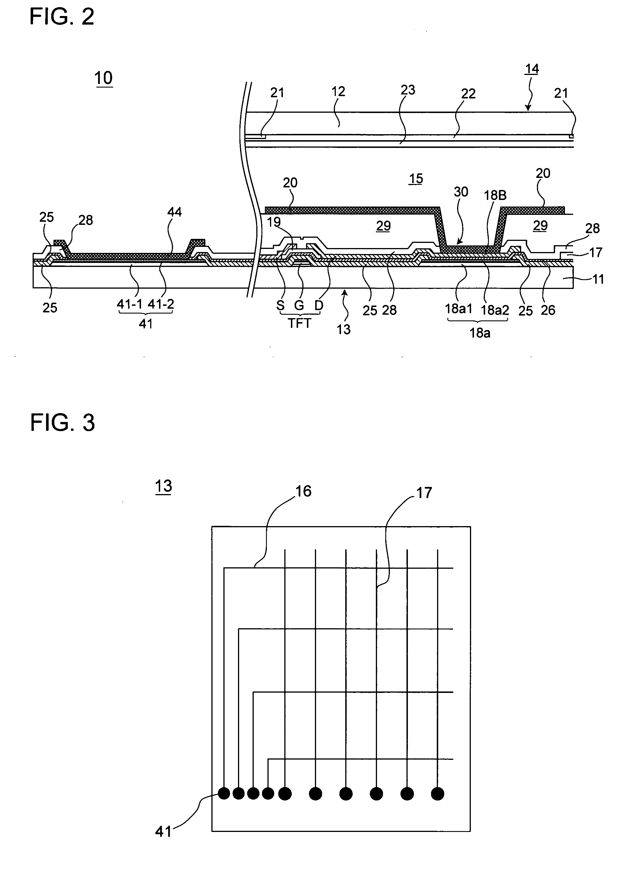
[0031]With the configuration described above, the liquid crystal display device according to the invention offers the following advantages. Since the second insulating film is formed as a dielectric layer of an auxiliary capacitance, it is possible to offer a large auxiliary capacitance while ensuring an adequate thickness of the first insulating film and the second insulating film that serve as a gate insulating film without increasing the area of an auxiliary capacitance forming region. This helps realize a liquid crystal display device that can increase the aperture ratio and reduce display trouble such as crosstalk or flicker. Additionally, in the terminal portion, since the edge of the opening in the first insulating film is coated with the second insulating film, the first insulating film is not present in the terminal portion. Thus, at the time of forming a terminal-portion contact hole in the terminal portion, it is possible to reduce the time to complete etching of the insulating film (the second insulating film and the third insulating film) laid on the terminal portion. This helps reduce the time during which the upper auxiliary capacitance electrode is exposed to an etching atmosphere, thereby reducing damage to the upper auxiliary capacitance electrode and the second insulating film laid under it.
[0032]Moreover, in the terminal-portion contact hole,
Problems solved by technology
This makes it practically difficult to provide a large auxiliary capacitance.
However, when the gate insulating film 75 itself is made thinner, it becomes difficult to maintain electrical isolation between the gate electrode G and the scanning line 72 that are coated with the gate insulating film 75 and other members.
However, it was found that just making thinner the gate insulating film laid on the surface of the auxiliary capacitance line cannot prevent a short circuit from easily occurring between the auxiliary capacitance electrode portion and an upper auxiliary capacitance electrode that is placed face to face with the auxiliary capacitance electrode portion.
Thus, even when etching of the insulating film laid on the upper auxiliary capac
Method used
View moreImage
Smart ImageViewing Examples

Examples
 PUM
 Abstract
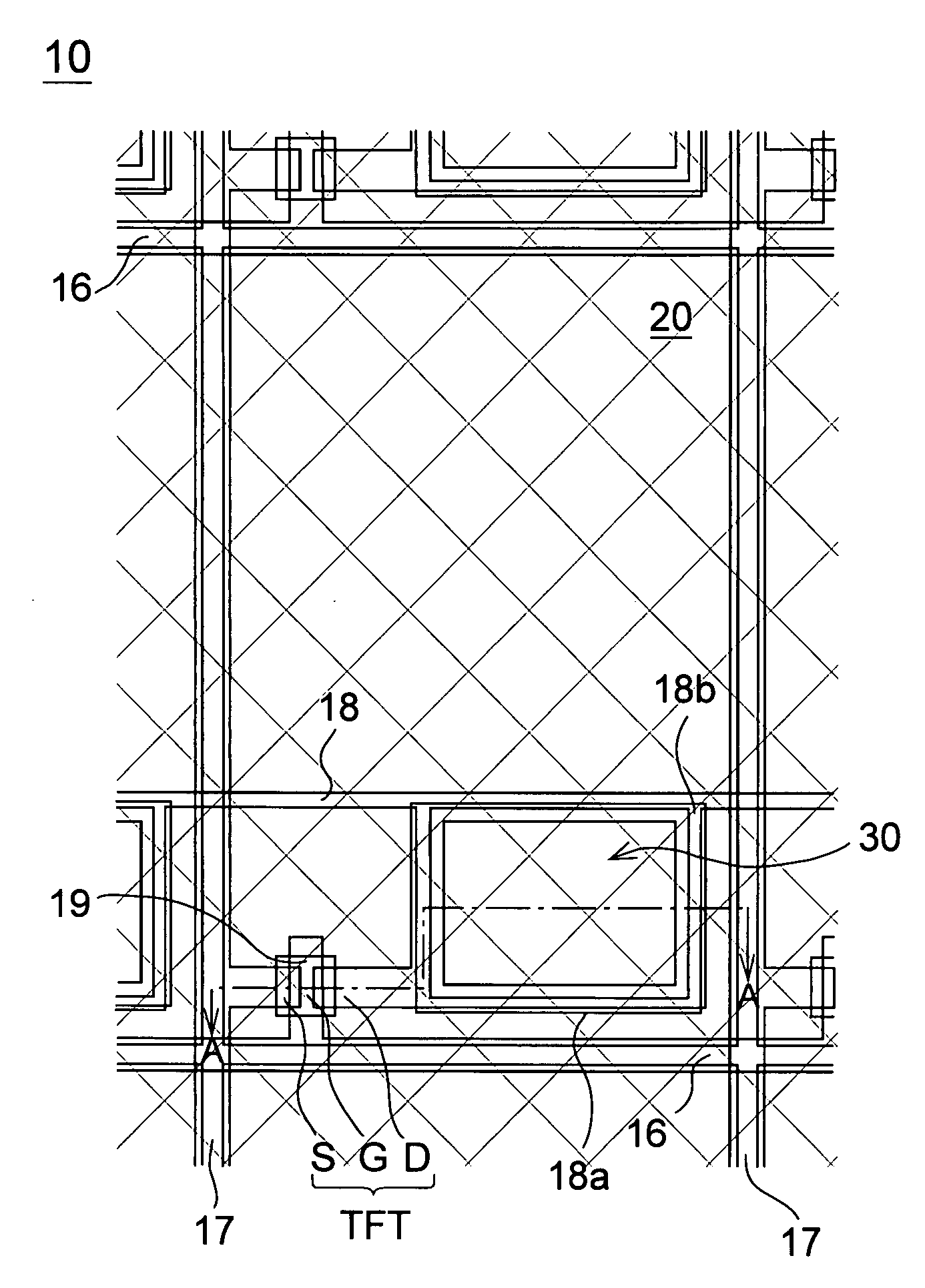
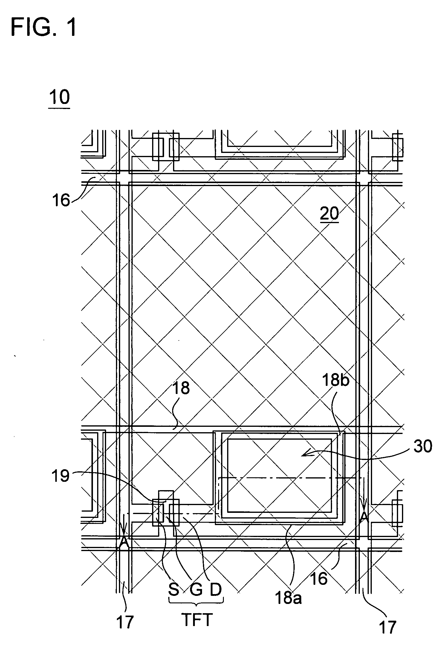
An auxiliary capacitance line and a terminal portion of a liquid crystal display device are made of an Al or Al alloy layer and an Mo layer. The edge portions of a lower auxiliary capacitance electrode and the terminal portion are sequentially coated with a first insulating film, a second insulating film that is thinner than the first insulating film, and a third insulating film. The lower auxiliary capacitance electrode is coated with the second insulating film, and an upper auxiliary capacitance electrode is laid on the surface of the second insulating film on the lower auxiliary capacitance electrode.
Description
[0001]This application is based on Japanese Patent Applications Nos. 2006-147713 and 2007-062949 filed on May 29, 2006 and Mar. 13, 2007 respectively, the contents of which are hereby incorporated by reference.BACKGROUND OF THE INVENTION[0002]1. Field of the Invention[0003]The present invention relates to liquid crystal display devices and manufacturing methods thereof. More particularly, the present invention relates to a liquid crystal display device that suffers less from a short circuit occurring in an auxiliary capacitance forming region, that can increase an auxiliary capacitance without reducing the aperture ratio of each pixel, and that is suitable for a relatively small pixel area or for achieving high definition, and relates to a manufacturing method of such a liquid crystal display device.[0004]2. Description of Related Art[0005]In recent years, liquid crystal display devices have come to be used widely not only in information communications apparatuses but also in common...
Claims
Login to View More Application Information
Patent Timeline
 IPC IPC(8): G02F1/1343
CPCG02F1/136227G02F1/136213G02F1/136
InventorNOMURA, SHINICHIROKATO, TAKAYUKIATARASHIYA, TAKAOSUGIYAMA, HIROKIMORITAI, SATOSHI
OwnerJAPAN DISPLAY WEST