Silicon controlled rectifier protection circuit

a rectifier protection and silicon technology, applied in the direction of basic electric elements, electrical equipment, semiconductor devices, etc., can solve the problems of large devices, scr cannot turn, and circuits such as telecommunication line card circuits are subject to harsh environments

Inactive Publication Date: 2007-12-06
SILICON LAB INC
View PDF2 Cites 6 Cited by
  • Summary
  • Abstract
  • Description
  • Claims
  • Application Information

AI Technical Summary

Benefits of technology

[0008]Another aspect of the present invention resides in a method for forming a p-well region on a substrate via implantation of a p-type dopant along a p-well region while blocking a portion of the p-well region, and forming an n-well region on the substrate adjacent the p-well region. In this way, a vertical junction between the n-well region and the p-well region may be formed that acts as a vertical junction of a lateral SCR. In one implementation, the method may be performed using a silicon on insulator (SOI) process in which an insulation layer is formed between a handle wafer region of the substrate and the n-well and p-well regions. The method may further include forming a circuit on the substrate that is to be protected from high voltage surges by the SCR.

Problems solved by technology

Various circuits such as telecommunication line card circuits are subjected to very harsh environments, as their terminals (i.e., tip and ring lines) extend from a central office to a subscriber location over telephone poles that are subject to lightning strikes and power crosses.
Further, the SCR cannot turn on during normal operation of the SLIC.
The need for lightly doped regions causes the devices to get large.
The lightly doped regions cause the resistivity to be high as well, making it difficult to achieve low on resistances without growing the device area to sizes that are not economical.
An obstacle preventing integration of these devices is that parasitic diodes and transistors turn on prematurely on negative-going transients that cause forward biasing of the substrate in junction-isolated processes.
This prevents proper operation of the SCR and prevents proper protection when used in a protection circuit.

Method used


Image

  • Silicon controlled rectifier protection circuit
  • Silicon controlled rectifier protection circuit
  • Silicon controlled rectifier protection circuit

Examples


Embodiment Construction

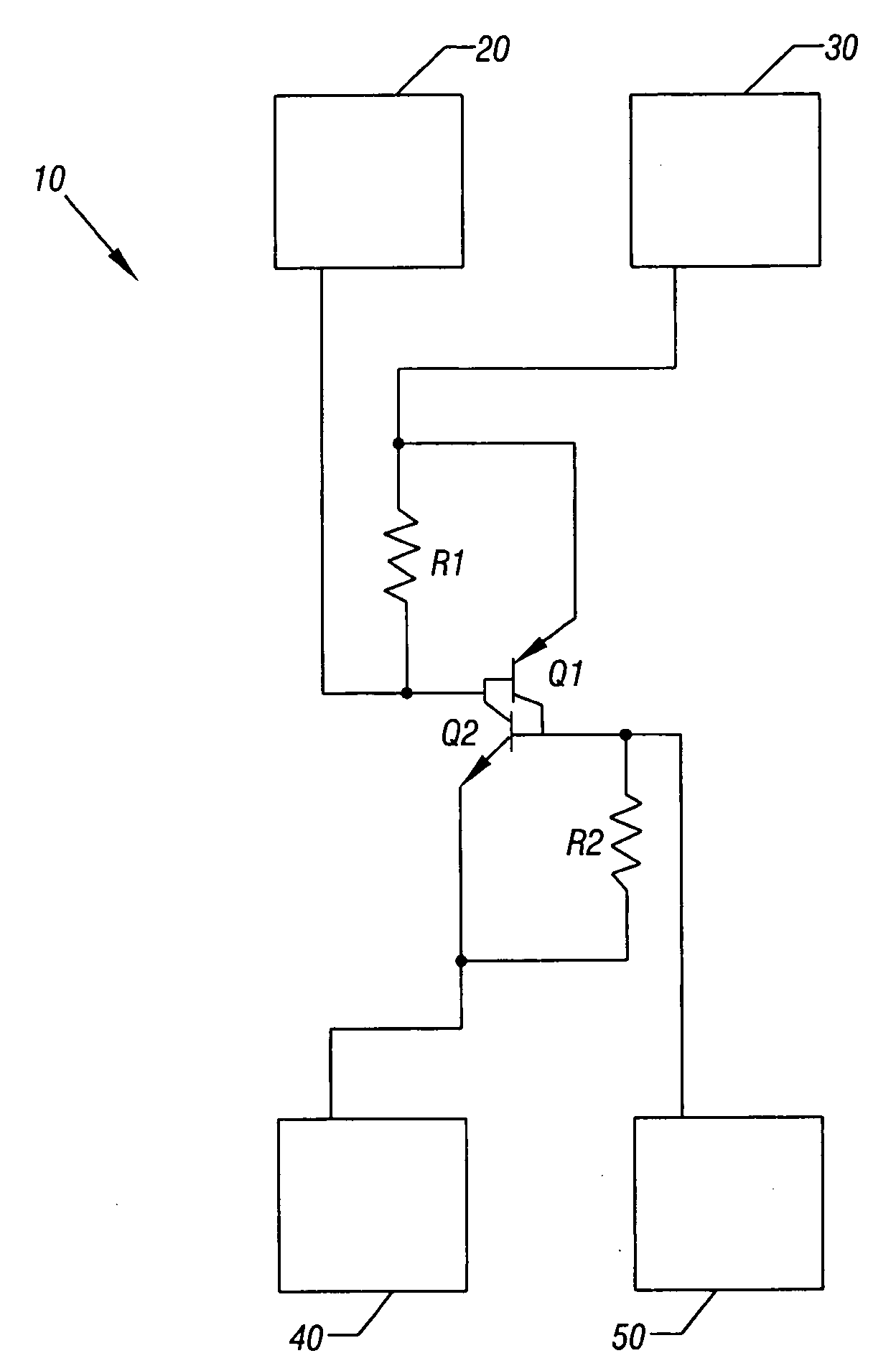
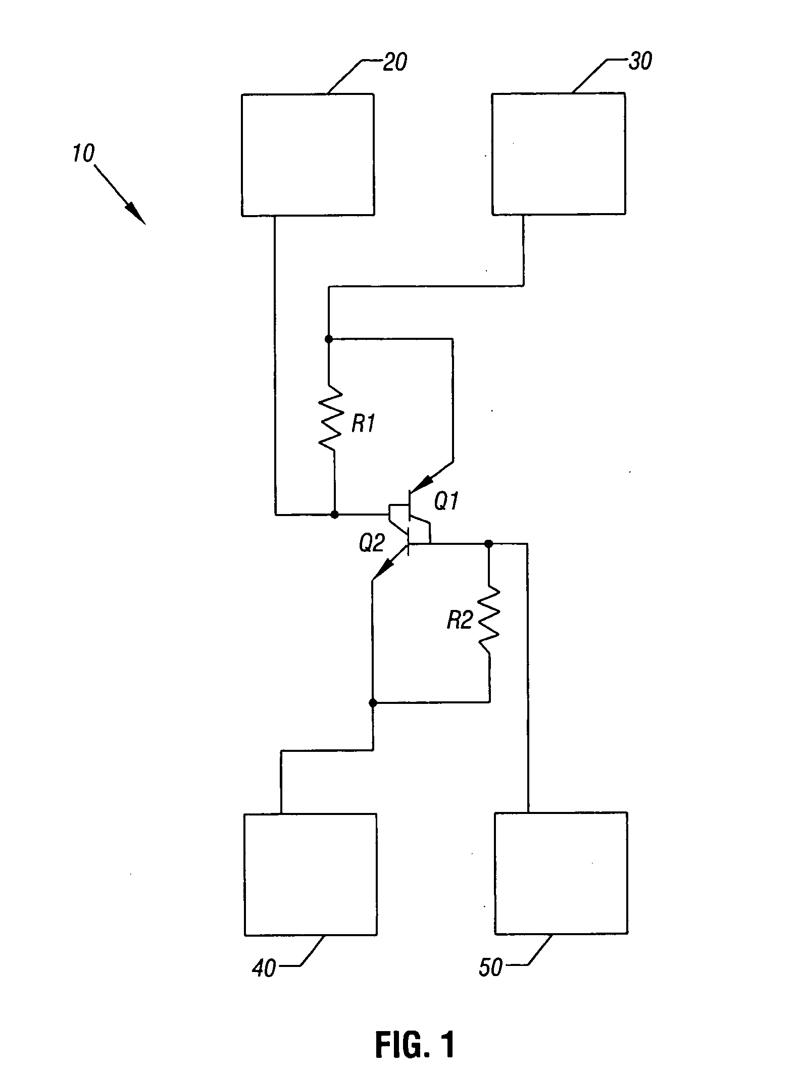
[0016]Referring now to FIG. 1, shown is a schematic diagram of a SCR in accordance with an embodiment of the present invention. As shown in FIG. 1, SCR 10 is formed of two transistors, namely a first transistor Q1 and a second transistor Q2. As shown in FIG. 1, first transistor Q1 may be a bipolar transistor, more specifically a PNP-type bipolar transistor, while second transistor Q2 may be an NPN-type bipolar transistor. As shown, the emitter of transistor Q1 is coupled to a bond pad 30, which may be an input / output (I / O) pin. Furthermore, the emitter is coupled to one end of a bypass resistor R1, for example, a 100 ohm resistor in one embodiment. The base of transistor Q1 is coupled to the other end of resistor R1 and another bond pad 20.

[0017]Still referring to FIG. 1, the collector of transistor Q1 is connected via a common or shared diffusion to the base of transistor Q2 and is further coupled to a second bypass resistor R2, which may also be a 100 ohm resistor, in one embodime...


PUM


Abstract

In one embodiment, the present invention includes an apparatus having a protection circuit to provide protection from transient surges. The protection circuit may include a silicon controlled rectifier (SCR) that is formed on a substrate via a planar process, along with one or more circuits to be protected by the protection circuit.

Description

FIELD OF THE INVENTION[0001]The present invention relates to an integrated circuit and more particularly to an integrated circuit including protection circuitry.BACKGROUND[0002]Various circuits such as telecommunication line card circuits are subjected to very harsh environments, as their terminals (i.e., tip and ring lines) extend from a central office to a subscriber location over telephone poles that are subject to lightning strikes and power crosses. This presents a need to protect the line card from damage due to lightning and power crosses. Protection of the line card is normally done in two stages. The first stage is a primary protection stage which drops the voltage down to a more manageable level (e.g., in the 1000V range). The second stage is a secondary protection stage which limits the voltage seen by the line card even further by shunting current to ground.[0003]The particular circuit being protected on a line card typically includes a circuit called a subscriber line i...

Claims


Application Information

Patent Timeline
Patent Type & Authority Applications(United States)
IPC IPC(8): H01L29/74
CPCH01L29/7436
Inventor HURST, ROGER S.
Owner SILICON LAB INC
Why Eureka
Try Eureka