Current sensor

a current sensor and sensor technology, applied in the direction of transformer/inductance details, inductances, instruments, etc., can solve the problems of inconvenient manufacturing and unstable welding, and achieve the effects of preventing dead space and unstable welding, fast manufacturing, and increasing welding spa

Inactive Publication Date: 2007-12-06
LIN TAI SHAN
View PDF2 Cites 12 Cited by
  • Summary
  • Abstract
  • Description
  • Claims
  • Application Information

AI Technical Summary

Benefits of technology

[0006]To figure out the shortcomings may express as follows: using an open of a C-type core of a current sensor to fasten a PCB directly, whereby the PCB is fast manufactured without drilling any welding hole. A contacting welding length of the C-type core and the PCB is longer for stronger support, and welding space is increased to prevent dead space and unstable welding so as to achieve easy manufacturing and fast and stable assembly. The PCB has a slot for a Hall sensing component being embedded therein by means of a plurality of bending portions of a plurality of terminals after the Hall sensing component connecting the PCB via such terminals. Therefore the entire thickness of the Hall sensing component is reduced, and the open of the C-type core is relatively smaller; further that, the magnetic flux impedance may be smaller due to the C-type core is closer to the Hall sensing component after assembling.

Problems solved by technology

On the other hand, the C-type core lies on the PCB by way of welding, and some dead spaces are not easy for welding so as to result in unstable welding and inconvenient manufacturing.

Method used


Image

  • Current sensor
  • Current sensor
  • Current sensor

Examples


Embodiment Construction

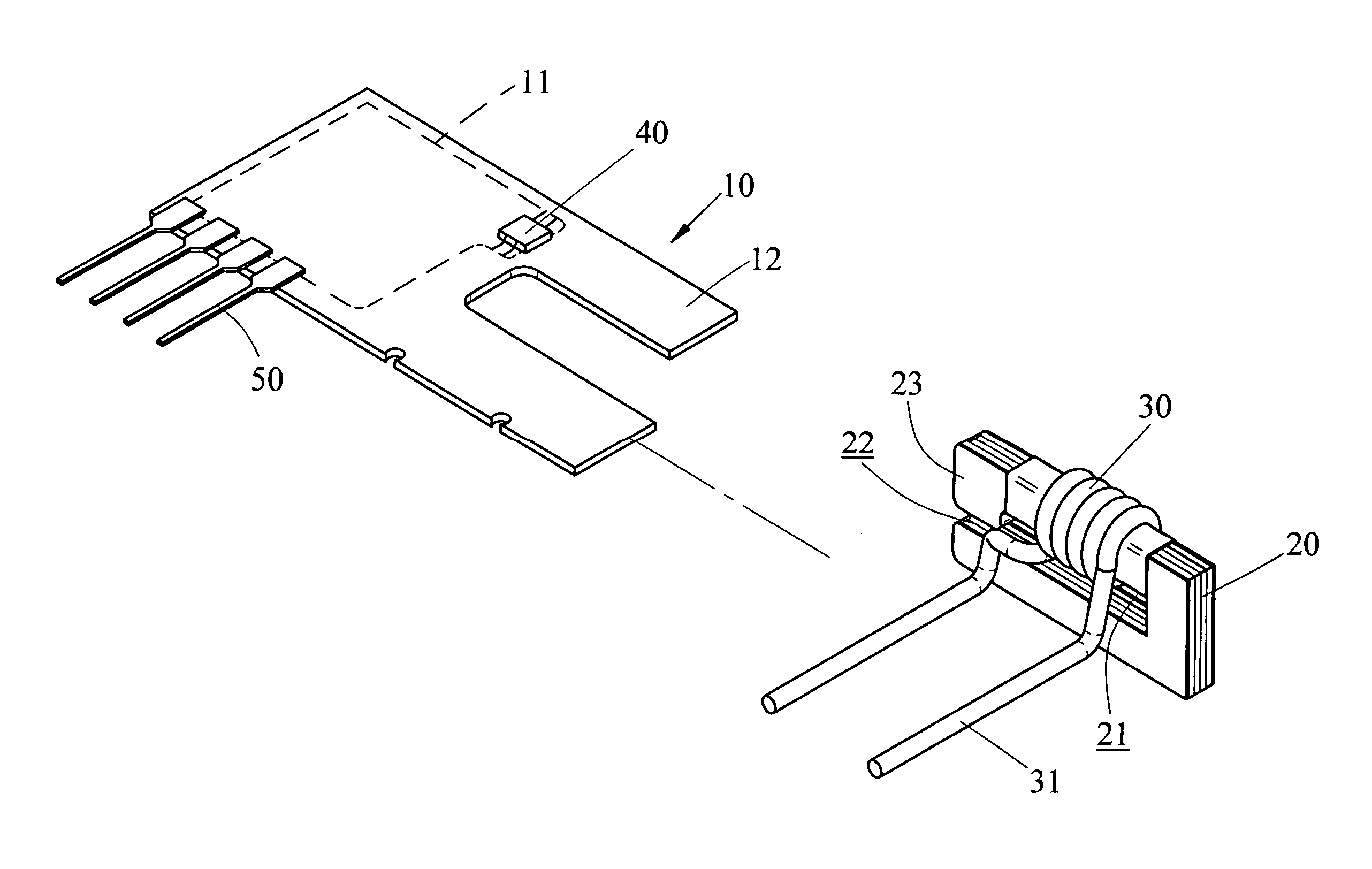
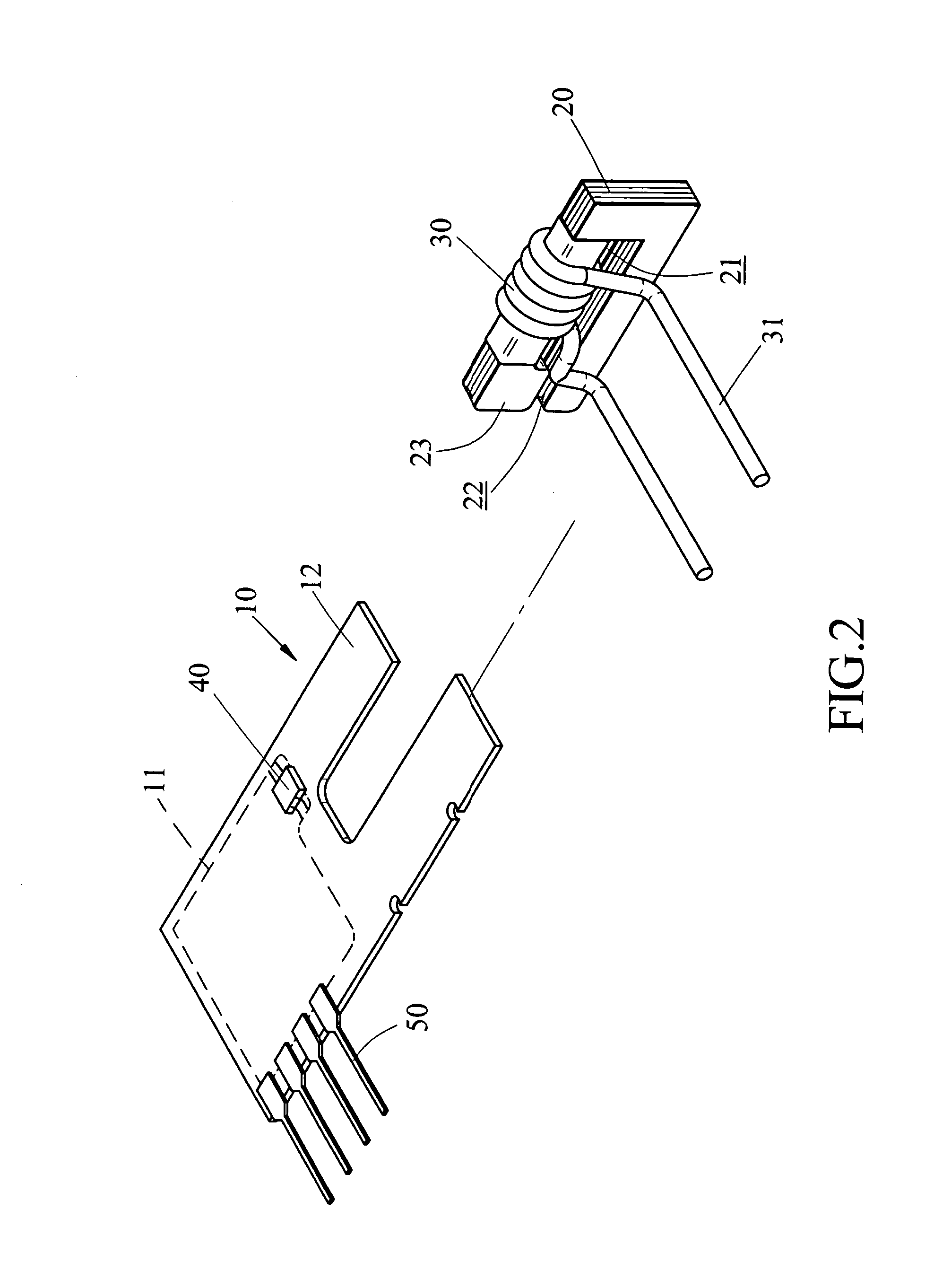
[0015]With reference to FIG. 2, which is a three-dimensional exploded view of a first preferred embodiment of the present invention. The current sensor of the present invention mainly comprises a PCB 10, a C-type core 20, a coil 30, a Hall sensing component 40, and a plurality of terminals 50; wherein the PCB 10 has an electric circuit 11 and the plurality of terminals 50 thereon, the terminals 50 elongate to outside along a direction parallel to the PCB 10 from the electric circuit 11, an elongating member 12 of the PCB 10 is protruded toward the C-type core 20, the Hall sensing component 40 is then welded on the electric circuit 11 of the PCB 10; the C-type core 20 opposite to the PCB 10 has an open 22, the open 22 forms an inner slot 21 inward, the C-type core 20 located on a side of the open 22 is a front bending portion 23; the coil 30 encircles the C-type core 20, two ends 31 of the coil 30 extend to outside of the PCB 10 for connecting and assembling other PCBs; the Hall sens...


PUM

PropertyMeasurementUnit
magnetic fieldsaaaaaaaaaa
circumferenceaaaaaaaaaa
lengthaaaaaaaaaa

Abstract

The present invention provides a current sensor, that is, an open of a C-type core of the current sensor is capable of fastening a PCB in order to dispose the core on the PCB perpendicularly. The PCB is then elongated to an inner surface of the core so as to firmly support the core and enlarge a welding area for the convenience of welding. A front bending portion of the core is properly opposite to a Hall sensing component, and a plurality of terminals of the Hall sensing component can be bended after welding to facilitate that the Hall sensing component embeds a slot of the PCB. Therefore, the advantages of easy manufacturing and fast and stable assembly is achieved; further that, the open of the C-type core is smaller, and the magnetic flux impedance may be smaller due to the C-type core is closer to the Hall sensing component.

Description

FIELD OF THE INVENTION[0001]The present invention is related to a current sensor, in particular to a sensor providing an open of a C-type core fastened a PCB directly, and contacting surfaces being welded, continuously a Hall sensing component being bended and embedded in slots of the PCB after welding so as to have a smaller open of the C-type core.BACKGROUND OF THE INVENTION[0002]A current sensor is mainly to convert magnetic fields to voltages, and such voltages can be amplified to controllable output voltages by means of electric circuits. With reference to FIG. 1, which is a plane schematic view of a current converter in prior arts. As shown in FIG. 1, the current converter with a flat figure primarily comprises a PCB 1, a C-type core 2, a coil 3, a Hall sensing component 4, and a plurality of terminals 6; wherein the PCB 1 has a plurality of circuits 5, the coil 3 encircles the C-type core 2, two ends 7 of the coil 3 elongate to outside of the PCB 1 for connecting other PCBs, ...

Claims


Application Information

Patent Timeline
Patent Type & Authority Applications(United States)
IPC IPC(8): H01F38/20
CPCG01R15/202G01R15/207H01F27/402H01F27/266H01F3/14
Inventor LIN, TAI-SHAN
Owner LIN TAI SHAN
Why Eureka
Try Eureka