Method for manufacturing wiring board

Active Publication Date: 2007-12-06
NGK SPARK PLUG CO LTD
View PDF5 Cites 63 Cited by
  • Summary
  • Abstract
  • Description
  • Claims
  • Application Information

AI Technical Summary

Problems solved by technology

However, because there is a large difference in pitch between the terminal block at the IC chip side and the terminal block at the motherboard side, it is difficult to directly connect the IC chip to the motherboard.
Since a length of the wiring connecting an IC chip and a capacitor becomes long, the above effect cannot be obtained due to an increase in ind

Method used


Image

  • Method for manufacturing wiring board
  • Method for manufacturing wiring board
  • Method for manufacturing wiring board

Examples


first embodiment

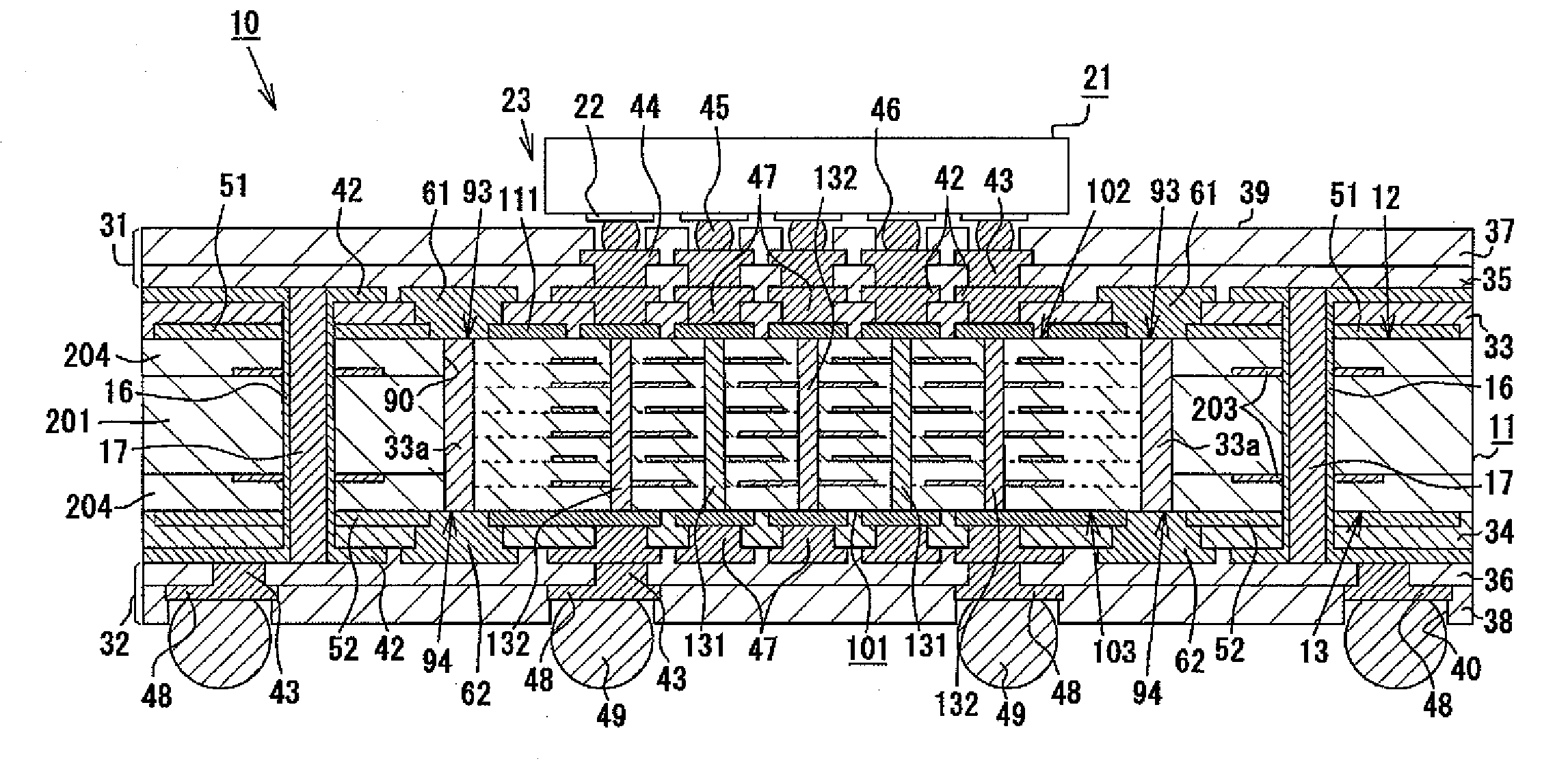
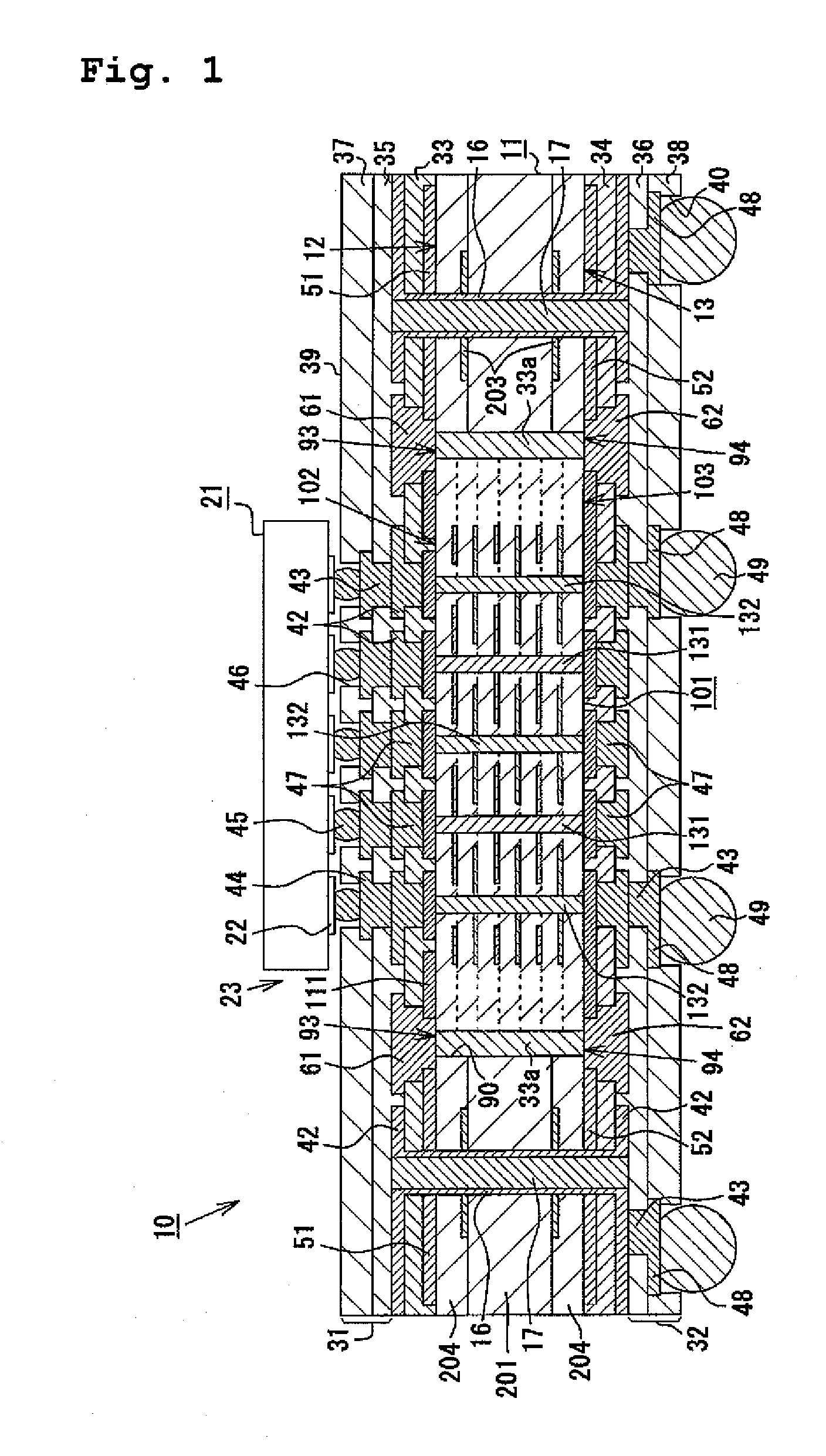
[0092]Hereafter, a first embodiment for carrying out a wiring board of the present invention will be described in detail with reference to the drawings.

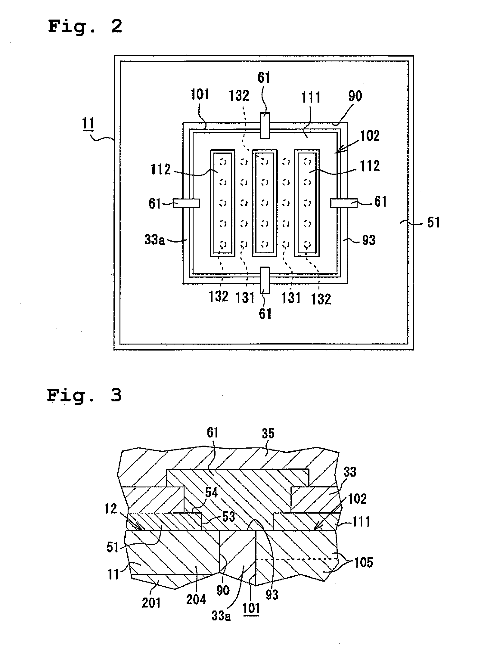
[0093]As shown in FIG. 1, a wiring board 10 according to this embodiment is a wiring board for mounting an IC chip and is composed of: a core board 11 assuming a generally rectangular form; a first wiring laminated body formed on a core main surface 12 (obverse surface in FIG. 1) of the core board 11; and a second wiring laminated body formed on a core rear surface 13 (reverse surface in FIG. 1) of the core board 11. The first wiring laminated body is composed of: a lowermost resin insulating layer 33 made of epoxy resin and constituting a lowermost layer of the first wiring laminated body; and a first buildup layer 31 formed on the lowermost resin insulating layer 33. On the other hand, the second wiring laminated body is composed of: an uppermost resin insulating layer 34 made of epoxy resin and constituting an uppermost layer of t...

second embodiment

[0132]Hereinafter, a wiring board according to a second embodiment of the invention will be described in detail with reference to the drawings.

[0133]As shown in FIGS. 19 and 20, a wiring board 10A according to the second embodiment uses a resin filler 92 different from that in the first embodiment where the resin filler 33a which constitutes a part of the lowermost resin insulating layer 33 is used for filling the gap between the inner face of the accommodation hole 90 and the side face of the ceramic capacitor 101. The resin filler 92 is made of polymer material (thermosetting resin, such epoxy, in this embodiment). Therefore, the method for manufacturing the wiring board 10A according to this embodiment also differs from that of the wiring board 10 according to the first embodiment.

[0134]In this embodiment, when the ceramic capacitor 101 is temporarily fixed in the accommodating hole 90, the fixing step is conducted, instead of forming the lowermost resin insulating layer 33 on th...


PUM


Abstract

A method for manufacturing a wiring board which can simplify a manufacturing step. In a preparation step, a core board and an electronic component are prepared. In an insulating layer formation and fixing step, after accommodating the electronic component in an accommodation hole, a lowermost resin insulating layer is formed, and a gap between the electronic component and the core board is filled with a part of the lowermost resin insulating layer so as to fix the electronic component to the core board. In an opening portion formation step, a portion of the lowermost resin insulating layer located directly above the gap between the electronic component and the core board is removed so as to form an opening portion exposing a part of a core board main surface side conductor and a component main surface side electrode. In a main surface side connecting conductor formation step, a main surface side connecting conductor is formed in the opening portion so as to connect the core board main surface side conductor to the component main surface side electrode.

Description

FIELD OF THE INVENTION[0001]The present invention relates to a wiring board having a structure in which an electronic component is embedded in a core board and a wiring laminated body is formed on a surface of the core board.BACKGROUND OF THE INVENTION[0002]In recent years, the semiconductor integrated circuit elements (IC chips) used for a CPU in a computer or the like operate at higher speeds, and with higher level functional features, than previously. Along with this advance, the number of terminals has increased and the terminal interval has tended to be smaller and narrower. Generally speaking, terminals in large numbers are densely packed on the bottom surface of the IC chip in an array, and a terminal block so formed is connected to a terminal block at the motherboard side by a “flip chip” connection. However, because there is a large difference in pitch between the terminal block at the IC chip side and the terminal block at the motherboard side, it is difficult to directly ...

Claims


Application Information

Patent Timeline
IPC IPC(8): H01L21/02
CPCH01L21/4857Y10T29/49155H01L23/49822H01L23/50H01L2224/16H01L2924/01078H01L2924/09701H01L2924/15311H05K1/0231H05K1/112H05K1/185H05K3/4602H05K2201/10674H05K2201/10712H01L2224/16235H01L23/13H01L2224/05573H01L2224/05568H01L2924/00014H01L2224/05599H01L23/12H05K3/30
Inventor KAWABE, TADAHIKOKURODA, MASAOSUGIMOTO, YASUHIROSAIKI, HAJIMEYURI, SHINJIORIGUCHI, MAKOTO
Owner NGK SPARK PLUG CO LTD
Why Eureka
Try Eureka