Peeling tape adhering method and peeling tape adhering device

Pending Publication Date: 2007-12-13
TOKYO SEIMITSU
View PDF2 Cites 19 Cited by
  • Summary
  • Abstract
  • Description
  • Claims
  • Application Information

AI Technical Summary

Benefits of technology

[0019]In the fifth and the sixth aspect, when the distance between the surface protection film and the peeling tape adhering means is reduced to a value not more than a predetermined value, the peeling tape adhering means is stopped from lowering. Therefore, it is easy to prevent fractures or cracks from being form on the entire wafer. Further, even in the case where the wafer is integrated with a mount frame into one body, the peeling tape adhering means is not pressed excessively. Therefore, it is possible t

Problems solved by technology

Thus, there is a possibility that fractures or cracks will

Method used


Image

  • Peeling tape adhering method and peeling tape adhering device
  • Peeling tape adhering method and peeling tape adhering device
  • Peeling tape adhering method and peeling tape adhering device

Examples


first embodiment

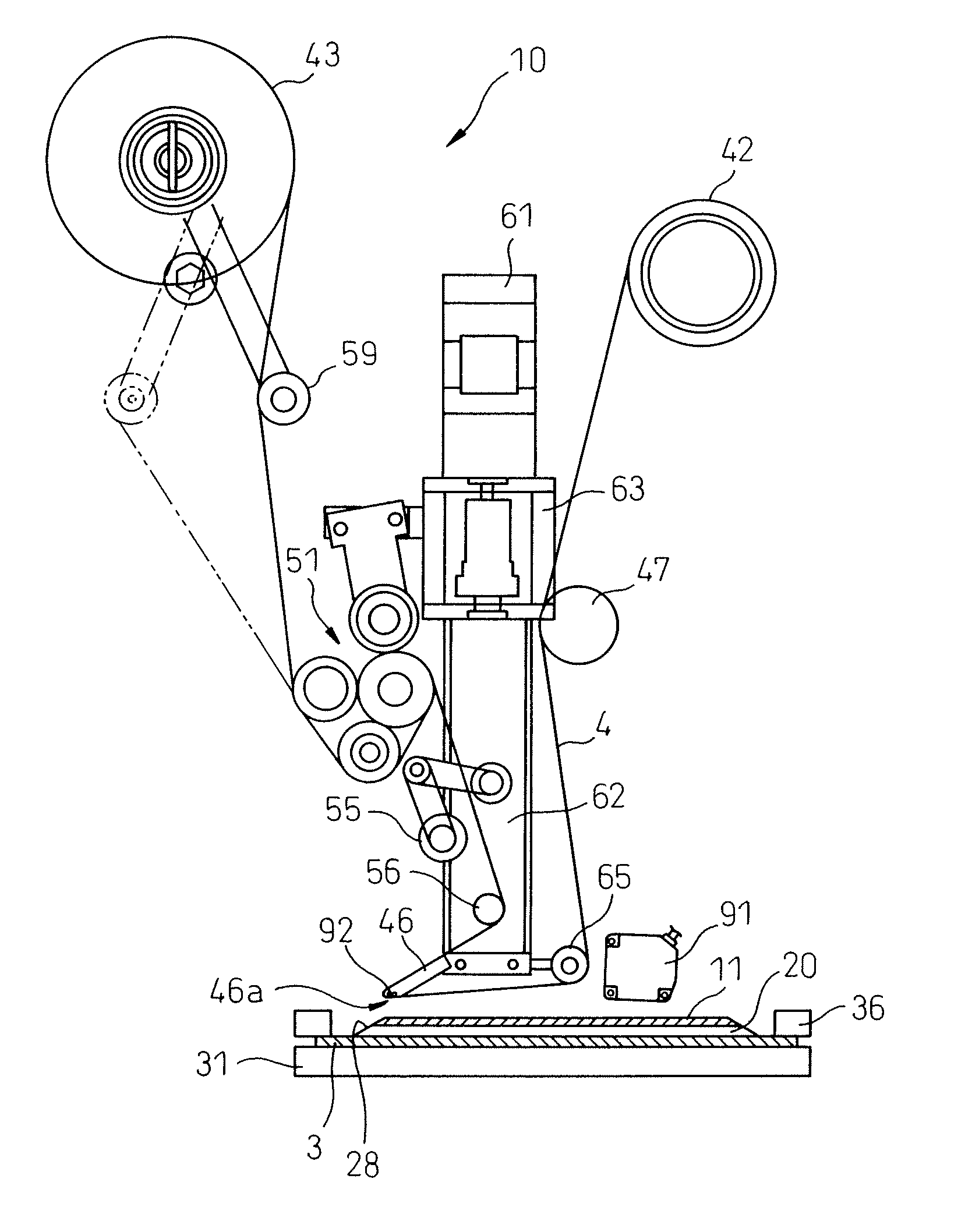
[0042]FIG. 3 is a flow chart showing an operation program of the surface protection film peeling device having the peeling tape adhering unit of the present invention. This operation program is incorporated into a memory of a control portion 95 (not shown) and executed by the control portion 95. In this connection, each element of the surface protection film peeling device 10 is connected to and controlled by the control portion 95.

[0043]FIGS. 4a, 4b, 5a and 5b are views explaining the operation of the surface protection film peeling device with the peeling tape adhering unit 60 of the present invention. So as to simplify the explanation, the distance sensor 91 is omitted from these drawings.

[0044]Referring to the drawings, the operation of the surface protection film peeling device 10 of the present invention will be explained below. In this connection, before the surface protection film peeling device 10 is driven, the peeling tape 4 has already been drawn out from the supply port...

second embodiment

[0056]FIG. 7 is a flow chart showing an operation program of a surface protection film peeling device having a peeling tape adhering unit of the present invention. Steps 201, 202, 205 and 206 of the operation program 200 shown in FIG. 7 are the same as steps 101, 102, 105 and 106 of the operation program 100 shown in FIG. 3. Therefore, explanations are omitted here.

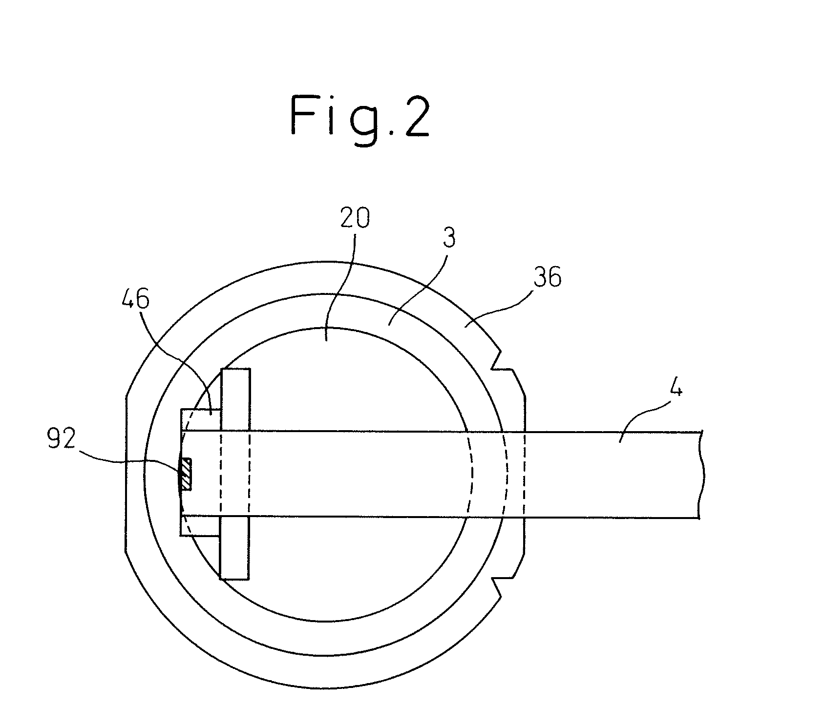
[0057]In step 203 shown in the operation program 200, distance L between the surface protection film 11 on the wafer 20 and the adhering member 46 is detected by the distance sensor 91 shown in FIG. 1. In step 204, the thus detected distance L is compared with the predetermined value L0. The predetermined value L0 is the distance between the surface protection film 11 and the adhering member 46 at which fractures or cracks or internal strain is not generated on the wafer 20. This predetermined value L0 was found through experiments, etc., and stored in the memory of the control portion 95. Specifically, this predetermined...


PUM

PropertyMeasurementUnit
Pressureaaaaaaaaaa
Distanceaaaaaaaaaa

Abstract

A peeling tap adhering method for adhering a peeling tape (4) to a surface protection film (11) adhered to the front surface of a wafer (20), comprises the steps of: supporting the wafer on a table (31) under the condition that the surface protection film is directed upward; adhering the peeling tape onto the surface protection film by pressing the peeling tape onto the surface protection film when a peeling tape adhering means (46) is lowered; detecting the pressure between the surface protection film of the wafer and the peeling tape adhering means; and stopping the peeling tape adhering means from lowering in the case where a pressure detection value (P) is not less than a predetermined value (P0). Due to the foregoing, it is possible to prevent the wafer from being cracked. Further, it is possible to prevent the peeling tape and the dicing tape from adhering to each other. When the distance (L) between the surface protection film of the wafer and the peeling tape adhering means becomes a value not more than a predetermined value (L0), the peeling tape sticking means may be stopped from lowering.

Description

BACKGROUND OF THE INVENTION[0001]1. Field of the Invention[0002]The present invention relates to a peeling tape adhering method for adhering a peeling tape to a surface protective film adhered on a wafer. The present invention also relates to a peeling tape adhering device for carrying out this peeling tape adhering method.[0003]2. Description of the Related Art[0004]In the field of manufacturing semiconductors, there is a tendency for large-sized wafers to be used year after year. Further, in order to enhance the packing density, the wafer thickness is reduced. In order to reduce the wafer thickness, back-grinding is conducted on the back surface of a semiconductor wafer. At the time of back-grinding, in order to protect a semiconductor element formed on the front surface of a wafer, a surface protection film is adhered to the front surface of the wafer.[0005]FIG. 8 is an enlarged sectional view showing a circular wafer onto which a surface protection film is adhered. As can be see...

Claims


Application Information

Patent Timeline
IPC IPC(8): B32B41/00B32B37/12
CPCH01L21/67132H01L21/08H01L21/302
Inventor KAWASHIMA, ISAMUSATO, HIDESHIKINO, HIDEOAMETANI, MINORU
Owner TOKYO SEIMITSU
Why Eureka
Try Eureka