Semiconductor Light Emitting Device

a technology of light-emitting devices and semiconductors, which is applied in the direction of semiconductor devices, basic electric elements, electrical equipment, etc., can solve the problems of increasing seriousness and the inability of all light-emitting units connected to a part of a series connection to operate, and achieve the effect of easy breakag

Inactive Publication Date: 2007-12-13
ROHM CO LTD
View PDF2 Cites 124 Cited by
  • Summary
  • Abstract
  • Description
  • Claims
  • Application Information

AI Technical Summary

Benefits of technology

[0026] By the present invention, in case that a semiconductor light emitting device of a monolithic type which can be operated with a commercial electric power source of, for example, 100 V is formed by dividing a semiconductor lamination portion into a plurality of light emitting units and by connecting between each of the light emitting units in series or parallel with a wiring film, since a separation groove separating each of the light emitting units is formed at a place where both surfaces of the semiconductor lamination portions in both sides of the separation groove are in a substantially same plane, there can be solved such problems as disconnection of the wiring film by a level difference caused by the separation groove and as less reliability of thin thickness even if the disconnection does not occur.
[0027] Namely, in the wiring film connecting between the light emitting units in series or parallel, since an electric connecting portion (which means a portion where the wiring film contacts to the semiconductor layer directly or through other conductor layer in an ohmic contact, and hereinafter referred to simply as electrode) connected to a semiconductor layer of a lower layer is at a low position, and an electrode connected to a semiconductor layer of an upper layer is at a high position, a level difference occurs in connecting the both electrode. In addition, when the separation groove is formed in order to separate electrically adjacent light emitting units, it is efficient to form the separation groove at a portion of a boarder from a surface of an exposed semiconductor layer of the lower layer. Therefor, since a large level difference is usu

Problems solved by technology

This problem becomes more serious if the number of the light emitting units increases.
Especially, in a case of a plenty of light emitting units connected in series, if disconne

Method used


Image

  • Semiconductor Light Emitting Device
  • Semiconductor Light Emitting Device
  • Semiconductor Light Emitting Device

Examples


Embodiment Construction

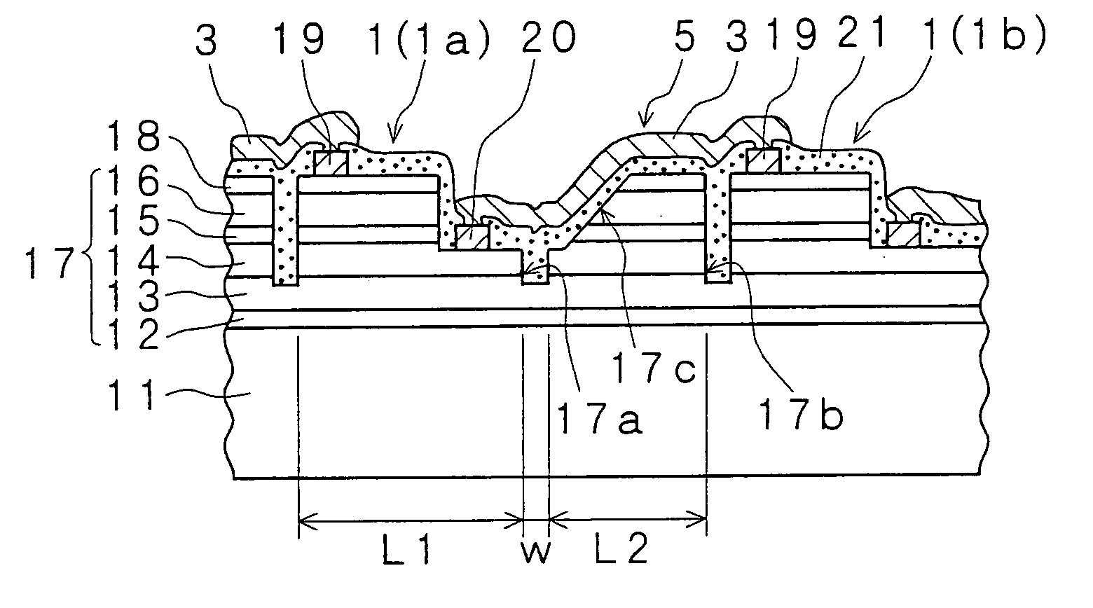
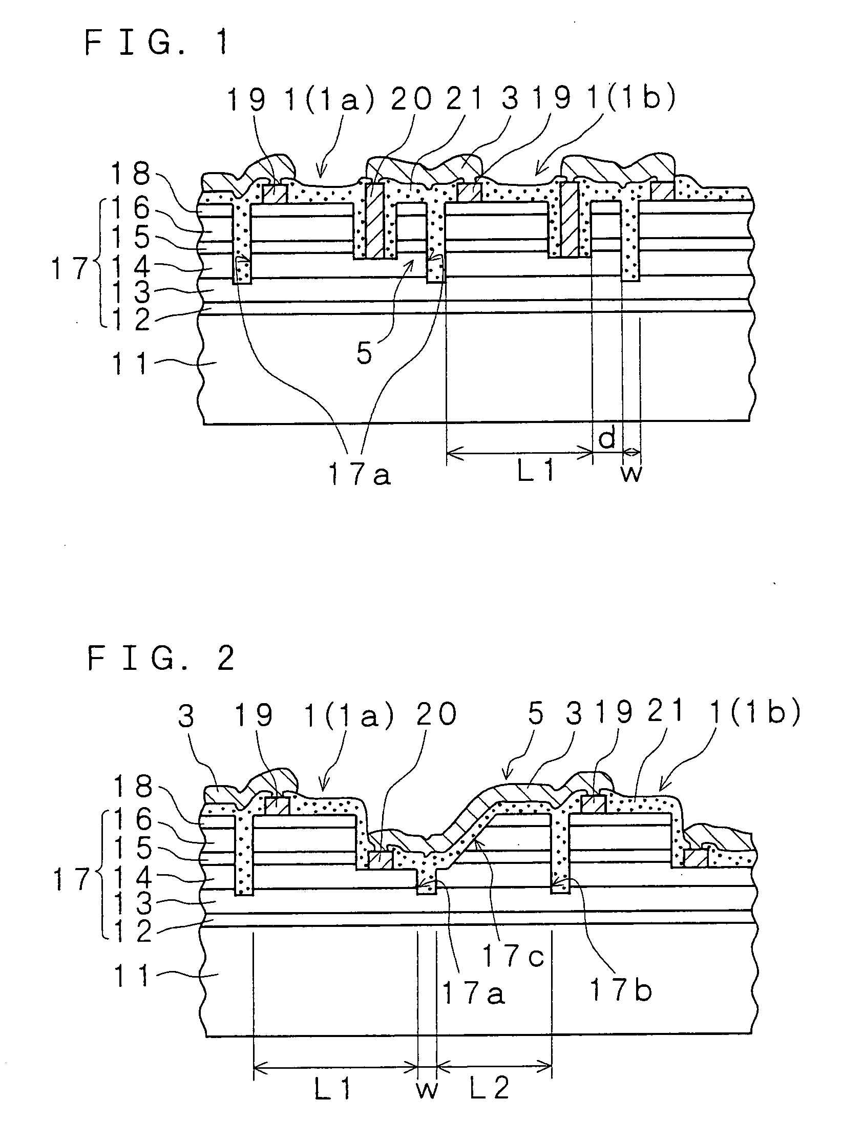
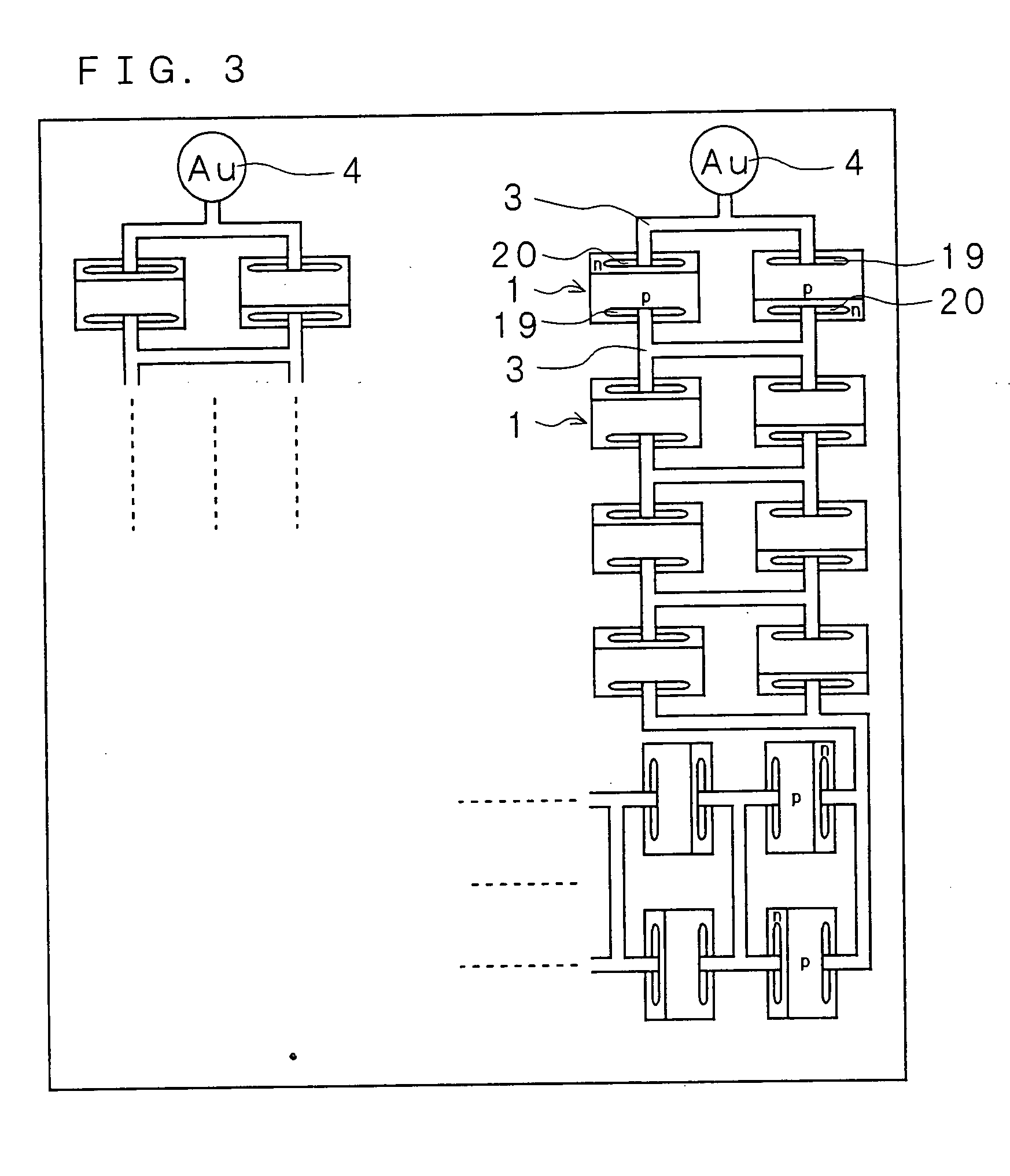
[0061] An explanation will be given below of a semiconductor light emitting device according to the present invention in reference to the drawings. As an explanatory cross-sectional view of one embodiment is shown, the semiconductor light emitting device according to the present invention is formed by forming a semiconductor lamination portion 17 on the substrate 11 by laminating semiconductor layers so as to form a light emitting layer, by forming a plurality of light emitting units 1 by separating the semiconductor lamination portion 17 electrically into a plurality of units 1, each of which has a pair of electric connecting portions (electrode 19 and 20) which are connected to a pair of conductivity type layers of the semiconductor lamination portion, respectively, and by connecting each of the plurality of light emitting units 1 in series and / or parallel with wiring films 3. In the present invention, a structure of electrically separating the plurality of light emitting units 1 ...


PUM


Abstract

There is provided a highly reliable semiconductor light emitting device in which disconnection of wires does not occur in case that a semiconductor light emitting device capable of being used in place of incandescent lamps or fluorescent lamps is formed in a monolithic type by forming a plurality of light emitting units on one substrate. A plurality of light emitting units (1) are formed by electrically separating a semiconductor lamination portion (17) which is so formed on a substrate (11) as to form a light emitting layer, and the light emitting units (1) are respectively connected in series and/or parallel by wiring films (3). For obtaining the light emitting units (1) from the semiconductor lamination portion a separation groove (17a) and an insulation film (21) deposited in the separation groove (17a) are formed in the semiconductor lamination portion (17). The separation groove (17a) is formed in such a position that the surfaces of the semiconductor lamination portion (17) on both sides of the separation groove (17a) are in the substantially same plane, and the wiring film (3) is formed on the separation groove (17a) through the insulating film (21).

Description

FIELD OF THE INVENTION [0001] The present invention relates to a semiconductor light emitting device in which a plurality of light emitting units are formed on a substrate and connected in series and / or parallel, and which can be used for light sources in place of incandescent lamps or fluorescent lamps used with commercial AC power sources of a voltage of, for example, 100 V. More particularly, the present invention relates to a semiconductor light emitting device which has a structure in which disconnection of a wiring film caused by a separation groove separating each of the light emitting units electrically hardly occurs, while connecting the plurality of light emitting units to each other with the wiring film provided on a top surface side of a semiconductor lamination portion. BACKGROUND OF THE INVENTION [0002] Being accompanied with developing blue light emitting diodes (LEDs), the LEDs are lately used for light sources of displays or traffic signals and furthermore become to...

Claims


Application Information

Patent Timeline
IPC IPC(8): H01L33/00H01L33/06H01L33/08H01L33/32H01L33/42H01L33/44H01L33/50
CPCH01L27/156H01L33/62H01L2924/0002H01L2924/00
Inventor SHAKUDA, YUKIONISHIDA, TOSHIOSONOBE, MASAYUKI
Owner ROHM CO LTD
Why Eureka
Try Eureka