Electrical Contactor, Espcecially Wafer Level Contactor, Using Fluid Pressure

a contactor and fluid pressure technology, applied in the direction of connection contact member materials, semiconductor/solid-state device testing/measurement, instruments, etc., can solve the problems of increased surface manufacturing costs, lack of contact, and difference in adequate flatness between the two surfaces

Inactive Publication Date: 2007-12-13
FORMFACTOR INC
View PDF99 Cites 37 Cited by
  • Summary
  • Abstract
  • Description
  • Claims
  • Application Information

AI Technical Summary

Problems solved by technology

In the case of the assemblies of FIGS. 1, 2, and 3, the wiring substrate is rigid in all three cases and thus any local differential in heights of the various contact elements (or other irregularities in the two opposing surfaces) may result in a lack of contact being made.
Such other irregularities may include a difference in adequate flatness between the two surfaces.
The requirement to control the flatness of the two surfaces also increases the manufacturing expense for the surfaces.
Furthermore, it is often difficult to achieve and maintain parallelism between the two surfaces, particularly. when incorporating the need for precise x, y positional alignment control which may restrict the ability to allow for a compensating tilt.

Method used


Image

  • Electrical Contactor, Espcecially Wafer Level Contactor, Using Fluid Pressure
  • Electrical Contactor, Espcecially Wafer Level Contactor, Using Fluid Pressure
  • Electrical Contactor, Espcecially Wafer Level Contactor, Using Fluid Pressure

Examples


Embodiment Construction

[0033] The present invention relates to interconnection assemblies and methods for making interconnections and particularly to interconnect assemblies and methods for making mechanical and electrical connection to contact elements on an integrated circuit. The following description and drawings are illustrative of the invention and are not to be construed as limiting the invention. Numerous specific details are described to provide a thorough understanding of the present invention. However, in other instances, well known or conventional details are not described in order to not unnecessarily obscure the present invention in detail.

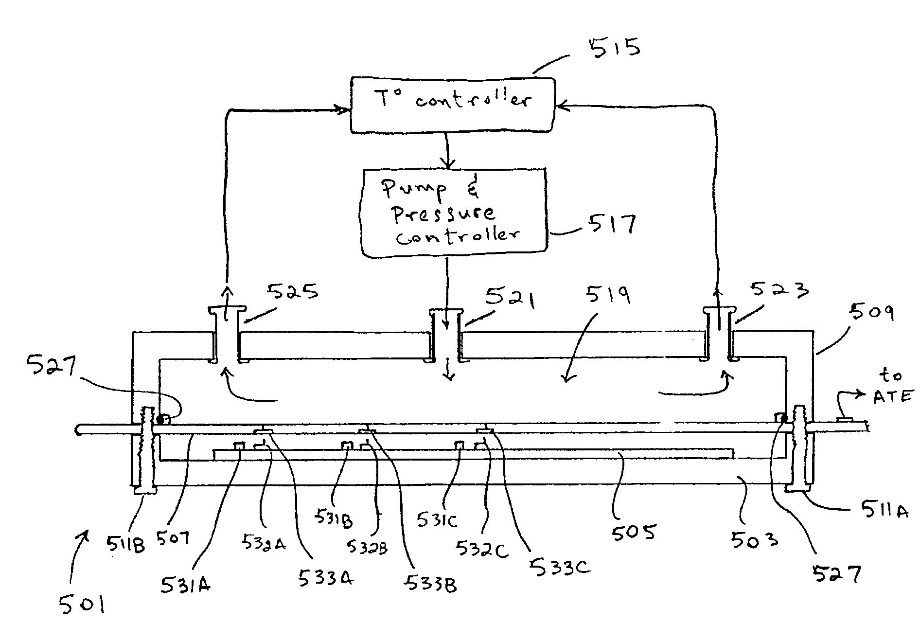
[0034]FIG. 5 shows one example of an electrical interconnection assembly according to the present invention. The assembly includes a fluid containing structure 509 which includes a chamber 519 for containing the fluid. The fluid is retained by the inner walls of the structure 509 and by the flexible wiring layer 507 which may, in one embodiment, be simila...


PUM


Abstract

An electrical interconnect assembly and methods for making an electrical interconnect assembly. In one embodiment, an interconnect assembly includes a flexible wiring layer having a plurality of first contact elements and a fluid containing structure which is coupled to the flexible wiring layer. The fluid, when contained in the fluid containing structure, presses the flexible wiring layer towards a device under test to form electrical interconnections between the first contact elements and corresponding second contact elements on the device under test. In a further embodiment, an interconnect assembly includes a flexible wiring layer having a plurality of first contact terminals and a semiconductor substrate which includes a plurality of second contact terminals. A plurality of freestanding, resilient contact elements, in one embodiment, are mechanically coupled to one of the flexible wiring layers or the semiconductor substrate and make electrical contacts between corresponding ones of the first contact terminals and the second contact terminals. In another embodiment, a method of making electrical interconnections includes joining a flexible wiring layer and a substrate together in proximity and causing a pressure differential between a first side and a second side of the flexible wiring layer. The pressure differential deforms the flexible wiring layer and causes a plurality of first contact terminals on the flexible wiring layer to electrically connect with a corresponding plurality of second contact terminals on the substrate.

Description

FIELD OF THE INVENTION [0001] The present invention relates to interconnect assemblies and methods for making and using interconnections and more particularly to interconnect assemblies for making electrical contact with contact elements on a substrate such as a semiconductor integrated circuit. More particularly, the present invention relates to methods and assemblies for making interconnections to semiconductor devices to enable test and / or burn-in procedures on the semiconductor devices. GROUND OF THE INVENTION [0002] There are numerous interconnect assemblies and methods for making and using these assemblies in the prior art. For example, it is usually desirable to test the plurality of dies (integrated circuits) on a semiconductor wafer to determine which dies are good prior to packaging them and preferably prior to being singulated from the wafer. To this end, a wafer tester or prober may be advantageously employed to make a plurality of discreet pressure connections to a like...

Claims


Application Information

Patent Timeline
Patent Type & Authority Applications(United States)
IPC IPC(8): H01R12/00G01R31/26G01R1/073G01R31/02G01R31/28G01R31/30H01L21/66H01R12/24
CPCG01R1/0735G01R31/2887G01R31/2886G01R1/073G01R31/316
Inventor ELDRIDGE, BENJAMIN N.
Owner FORMFACTOR INC
Why Eureka
Try Eureka