
Eureka
For R&D, Eureka makes reading and utilizing patents & technical documents easy.
Eureka AIR
Designed for self-driven R&D workflows. Generate viable solutions, solve complex R&D challenges, empower your innovation with AI.

Eureka Materials
Designed for material experts only. Revolutionize your material R&D, from search, analyze, to developing new materials.

TechResearch
Generate reliable direction feasibility study reports for your R&D in just a few steps.

TechSeek
Discover and master advanced knowledge NOW. Basics, ideas, possibilities, all at once.

TechMind
As an expert in R&D Theories, TechMind can generates customized viable solutions instantly.

TechRisk
Analyze your overall solution with one click, know your potential R&D risks in advance.

TechMonitor
Get weekly tech updates, stay abreast of the latest tech innovations and key insights.
Stacking structure of chip package
- Summary
- Abstract
- Description
- Claims
- Application Information
AI Technical Summary
Benefits of technology
Problems solved by technology
Method used
Image

Examples
Embodiment Construction
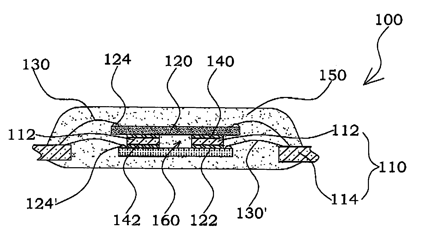
[0020]Please refer to FIG. 4A and FIG. 4B, are the top plan view and sectional view diagram illustrating the stacking structure of chip package in accordance with an embodiment of the present invention respectively. As shown in FIG. 4A, the stacking structure of chip package 100 includes a first chip 120, a second chip 122, a lead frame 110, an electrical-connecting element 130, 130′ and a molding compound 150 (shown in FIG. 4B). The lead frame 110 having a plurality of supporting fingers 112 and a plurality of leads 114; a first chip arranged on one side of the lead frame 110, such as the one side between the first chip 120 and the supporting finger 112, by utilizing a first connecting element with known skill, such as, plaster, and partially covered supporting finger 112 wherein the supporting finger 112 stretch from the edge of the first chip 120 toward the first chip 120 so as to provide a support. And a second chip 122 arranged on the opposite side of the position of the first ...
PUM
 Abstract
Description
Claims
Application Information
 - R&D Engineer
- R&D Manager
- IP Professional
- Industry Leading Data Capabilities
- Powerful AI technology
- Patent DNA Extraction
Browse by: Latest US Patents, China's latest patents, Technical Efficacy Thesaurus, Application Domain, Technology Topic, Popular Technical Reports.
© 2024 PatSnap. All rights reserved.Legal|Privacy policy|Modern Slavery Act Transparency Statement|Sitemap|About US| Contact US: help@patsnap.com