

Grounding strategy for filter on planar substrate
a filter and substrate technology, applied in the direction of electrical equipment, multiple-port networks, waveguides, etc., can solve the problems of deteriorating filter performance, increasing the cost of etching process, slow process for creating via holes, etc., to reduce the feedback effect and reduce the deterioration of filter outband rejection performance caused by common ground inductan
- Summary
- Abstract
- Description
- Claims
- Application Information
AI Technical Summary
Benefits of technology
Problems solved by technology
Method used
Image

Examples
Embodiment Construction
[0001]1. Field of the Invention
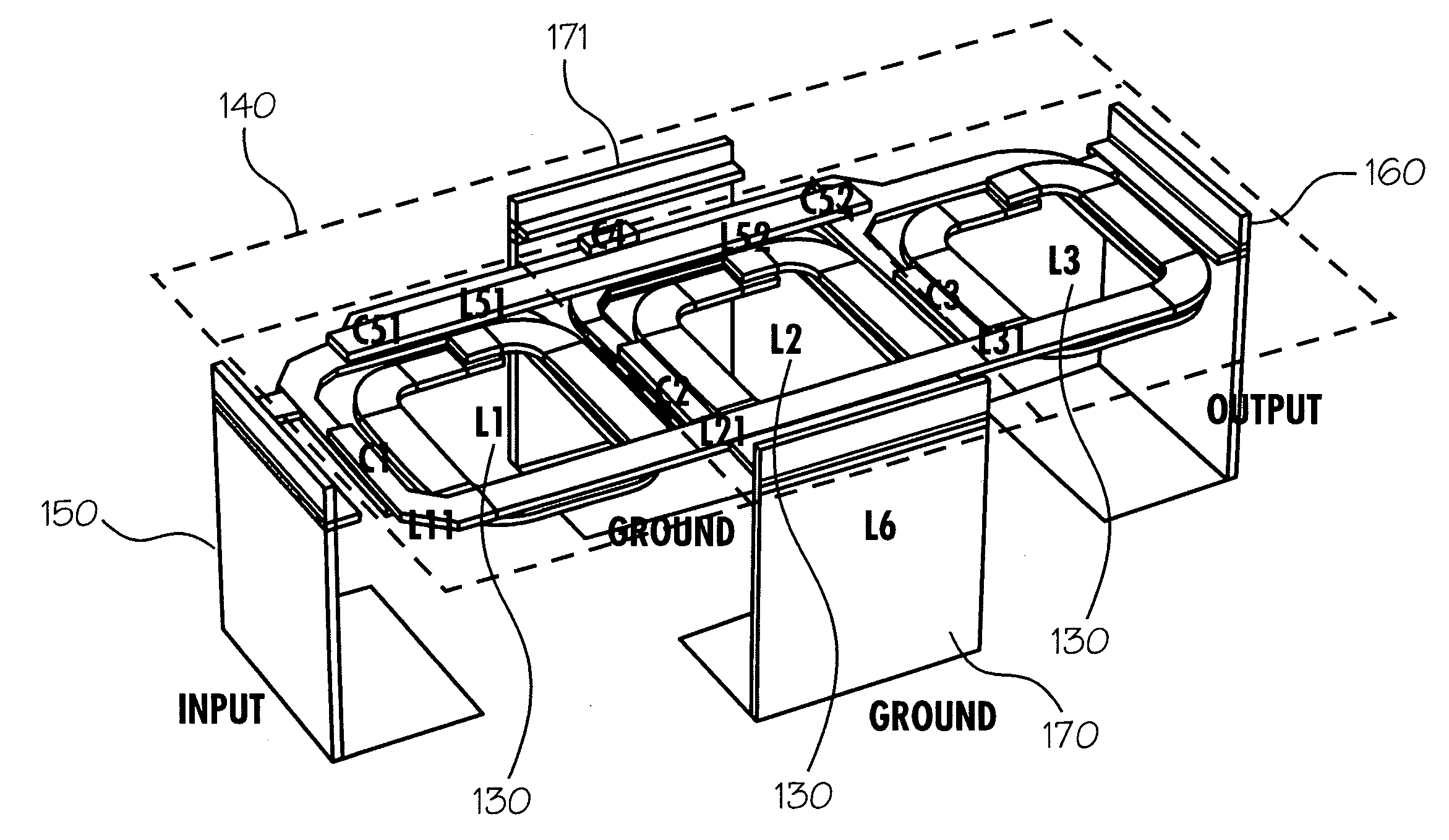
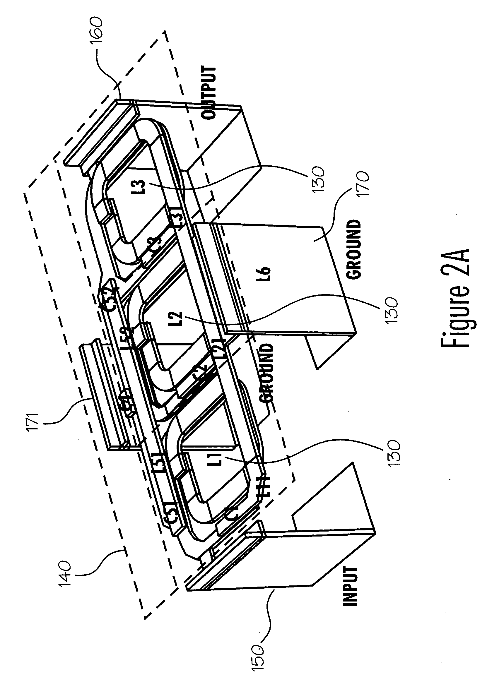
[0002]The present invention relates to a grounding strategy for electronic components, and more specifically to a ground strategy for filters on a planar substrate.
[0003]2. Background of the Invention
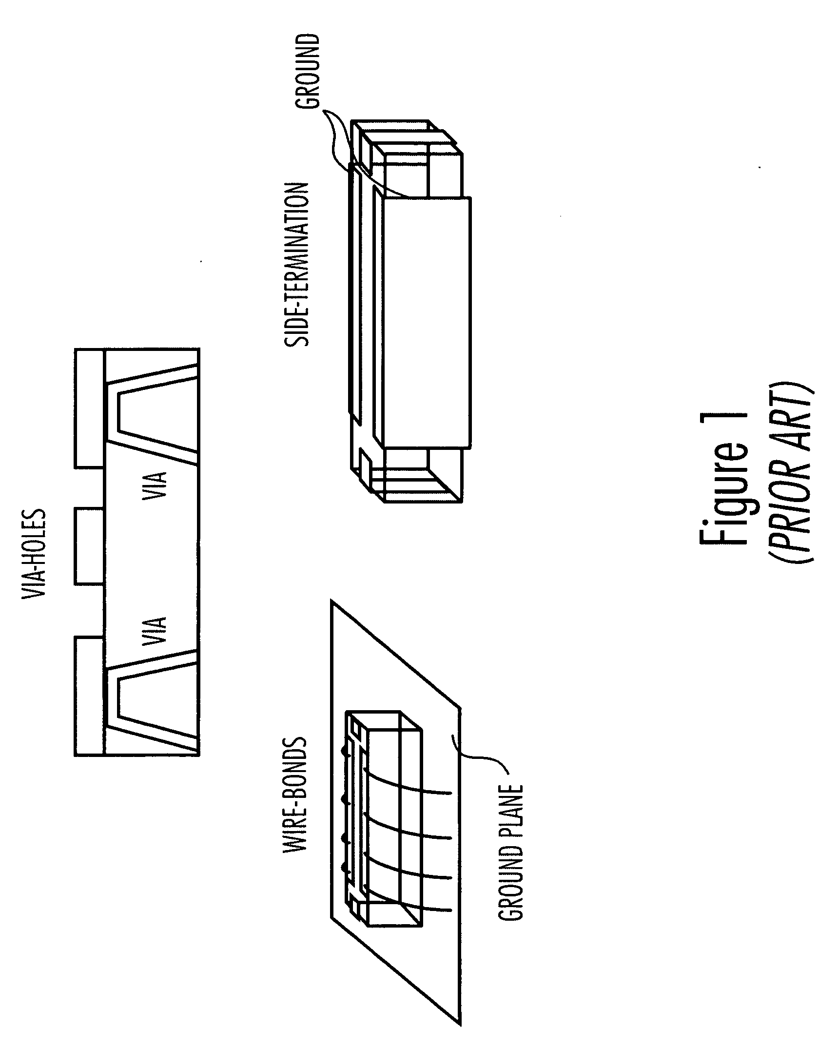
[0004]Electronic components, and particularly electronic filters, built on substrates using microstrip or stripline technology often have on-chip circuit ground connected to a system ground plane at a different level of the chip substrate. Conventionally, without using complex flip-chip technology developed in recent years, these ground connections can be realized with via-holes, bond-wires or side-wall metallic terminations, as is shown in FIG. 1. In filter applications, these ground connections bring associated parasitic inductance which may deteriorate filter performance; especially at upper stop-bands since parasitic inductance more greatly affects higher frequency signals. This is due to the proportional relationship between inductor reactance and fre...
PUM
 Abstract
Description
Claims
Application Information