Grounding strategy for filter on planar substrate

a filter and substrate technology, applied in the direction of electrical equipment, multiple-port networks, waveguides, etc., can solve the problems of deteriorating filter performance, increasing the cost of etching process, slow process for creating via holes, etc., to reduce the feedback effect and reduce the deterioration of filter outband rejection performance caused by common ground inductan

Active Publication Date: 2009-05-12
TDK CORPARATION
View PDF12 Cites 7 Cited by
  • Summary
  • Abstract
  • Description
  • Claims
  • Application Information

AI Technical Summary

Benefits of technology

[0004]In view of the foregoing, the invention provides a grounding strategy for electronic components. In particular, the present invention reduces feedback effect associated with common ground connections in thin-film electronic components by connecting one group of one or more resonators to one ground connection and connecting a second group of one or more resonators to another ground connection. This strategy reduces the feedback effect of the common ground inductance to all resonators. The filter outband rejection performance deterioration caused by common ground inductance is reduced. Due to this separate ground path, additional transmission zeros may be generated in the stop-band and can be individually tuned to frequency locations where maximum attenuations are desired.
[0005]According to one embodiment, the invention provides an electronic component that includes a first group of one or more resonators located in a first group of two or more thin-film layers, a second group of one or more resonators located in a second group of two or more thin-film layers, a first ground connection, and a second ground connection. Each resonator in the first group of one or more resonators is connected to the first ground connection and each resonator in the second group of one or more resonators is connected to the second ground connection. In this way, interference among resonators caused by parasitic ground inductance of the electronic component may be reduced and performance of the component improved.

Problems solved by technology

In filter applications, these ground connections bring associated parasitic inductance which may deteriorate filter performance; especially at upper stop-bands since parasitic inductance more greatly affects higher frequency signals.
However, the process for creating via holes is slow and expensive especially for etching processes.
However, additional wire-bonds need enlarged bonding pad surfaces and access room to the pads.
Consequently the number of possible ground connections is limited.

Method used


Image

  • Grounding strategy for filter on planar substrate
  • Grounding strategy for filter on planar substrate
  • Grounding strategy for filter on planar substrate

Examples


Embodiment Construction

[0034]Reference will now be made in detail to the present exemplary embodiments of the invention, examples of which are illustrated in the accompanying drawings.

[0035]The present invention provides a grounding strategy for electronic component, and in particular, a grounding strategy for filters having a planar substrate. For example, this grounding strategy is applicable for use electronic components constructed with any thin-film technique.

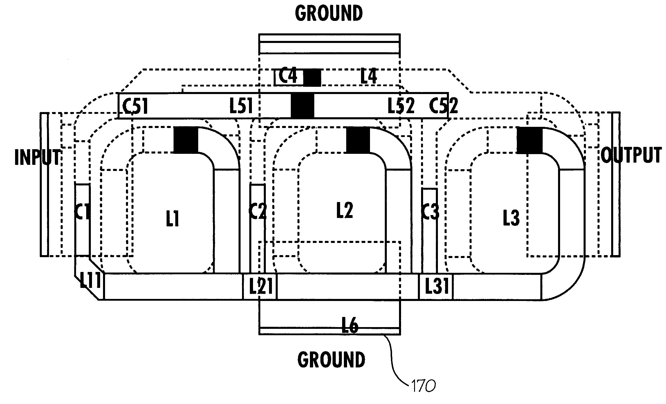
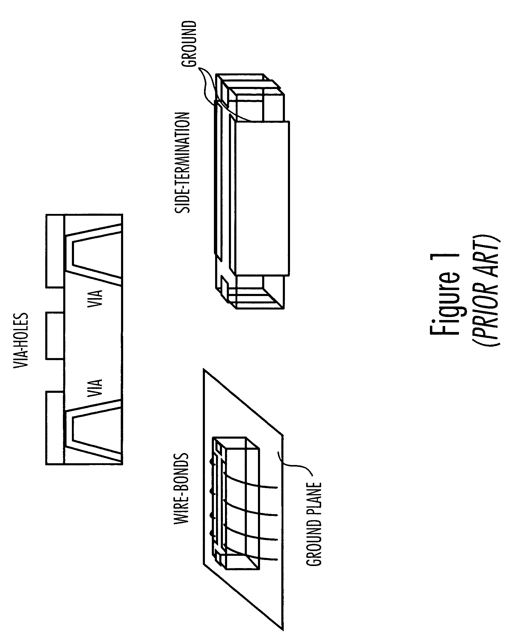
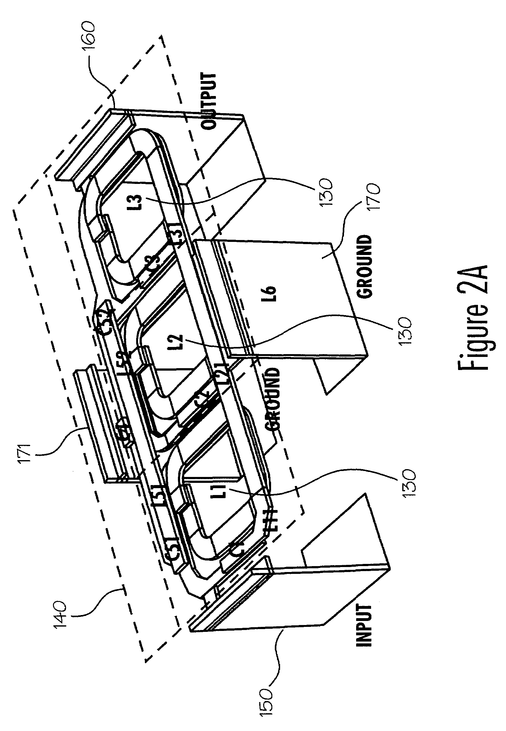
[0036]Conventional thin-film filters with side-wall terminations typically exhibit a ground inductance of approximately 0.16 nH for a housing size of 1 mm by 0.5 mm and a substrate thickness of 0.3 mm. FIGS. 2a and 2b show an example structure of such a bandpass filter with three resonators and FIG. 3 shows its circuit schematic diagram. The bandpass filter in FIG. 2a has three LC resonators 130 each connected to ground 170 through inductor L6. Ground 170 is configured as a sidewall termination. Three additional sidewall terminations function as...


PUM


Abstract

The invention provides a grounding strategy for electronic components. In particular, the present provides ground connections in thin-film electronic components by connecting one group of one or more resonators to one ground connection and connecting a second group of one or more resonators to another ground connection.

Description

FIELD OF THE INVENTION[0001]The present invention relates to a grounding strategy for electronic components, and more specifically to a ground strategy for filters on a planar substrate.BACKGROUND OF THE INVENTION[0002]Electronic components, and particularly electronic filters, built on substrates using microstrip or stripline technology often have on-chip circuit ground connected to a system ground plane at a different level of the chip substrate. Conventionally, without using complex flip-chip technology developed in recent years, these ground connections can be realized with via-holes, bond-wires or side-wall metallic terminations, as is shown in FIG. 1. In filter applications, these ground connections bring associated parasitic inductance which may deteriorate filter performance; especially at upper stop-bands since parasitic inductance more greatly affects higher frequency signals. This is due to the proportional relationship between inductor reactance and frequency.[0003]In vi...

Claims


Application Information

Patent Timeline
Patent Type & Authority Patents(United States)
IPC IPC(8): H01P1/20H01P3/08
CPCH01P1/20381
Inventor CHEN, QIANG RICHARD
Owner TDK CORPARATION
Why Eureka
Try Eureka