Data strobe signal generator for generating data strobe signal based on adjustable preamble value and semiconductor memory device with the same

a data strobe signal and data technology, applied in the field of semiconductor memory devices, can solve the problems of difficult to ensure a stabilization time, the data output circuit cannot normally output data, and the pulse width of the data strobe signal is not uniform, so as to achieve the effect of stabilizing the data output operation

Inactive Publication Date: 2007-12-20
SK HYNIX INC
View PDF7 Cites 33 Cited by
  • Summary
  • Abstract
  • Description
  • Claims
  • Application Information

AI Technical Summary

Benefits of technology

[0004]Accordingly, the present invention has been made keeping in mind the above problems occurring in the prior art, and an object of the present invention is to provide a data strobe sig

Problems solved by technology

The reason for this is that the pulse width of the data strobe signal is not uniform during an initial interval during which the strobe signal starts to toggle.
If the pulse width of the data strobe signal is not uniform, the data output circui

Method used


Image

  • Data strobe signal generator for generating data strobe signal based on adjustable preamble value and semiconductor memory device with the same
  • Data strobe signal generator for generating data strobe signal based on adjustable preamble value and semiconductor memory device with the same
  • Data strobe signal generator for generating data strobe signal based on adjustable preamble value and semiconductor memory device with the same

Examples


Embodiment Construction

[0015]Reference now should be made to the drawings, in which the same reference numerals are used throughout the different drawings to designate the same or similar components.

[0016]Preferred embodiments of the present invention are described below with reference to the accompanying drawings.

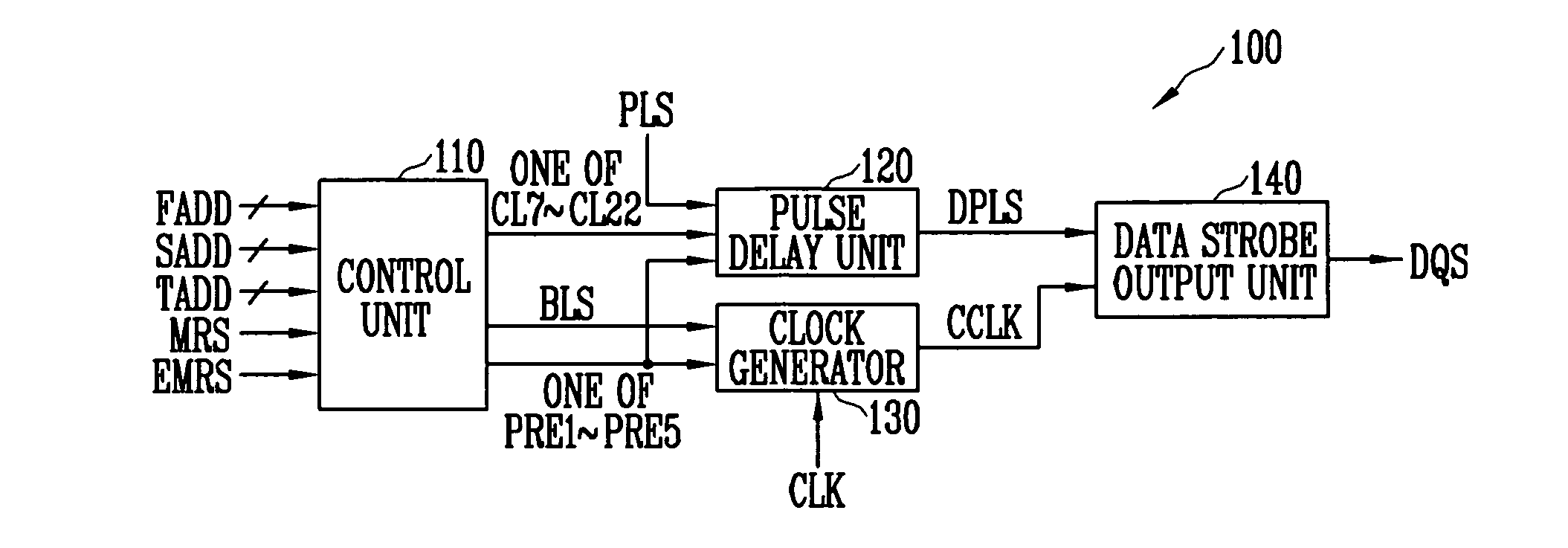
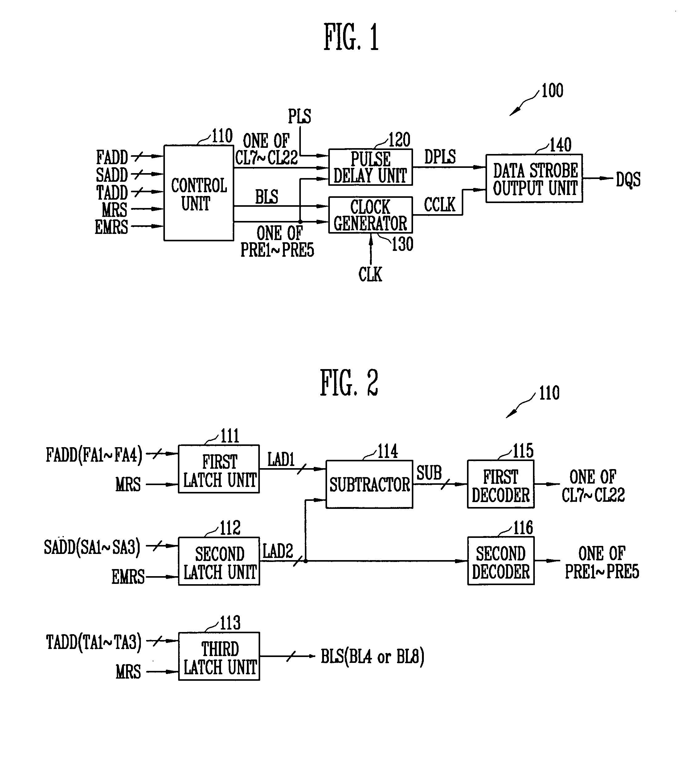
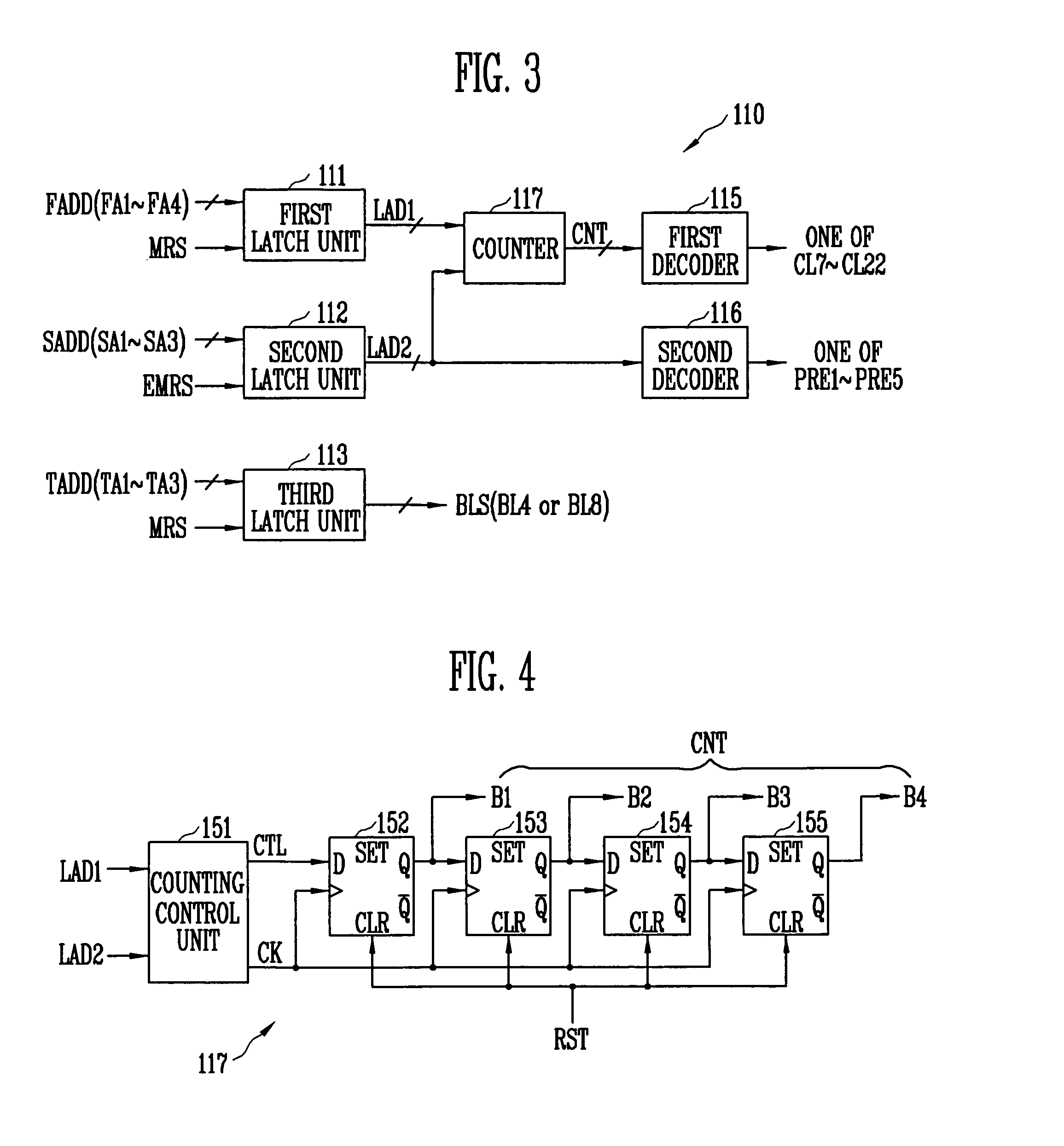
[0017]FIG. 1 is a block diagram illustrating a data strobe signal generator according to an embodiment of the present invention. Referring to the FIG. 1, the data strobe signal generator 100 includes, a control unit 110, a pulse delay unit 120, a clock generator 130, and a data strobe output unit 140. The control unit 110 generates one of CAS latency signals CL7˜CL22 and one of preamble signals PRE1˜PRE5 in response to a mode register set signal MRS, an extended mode register set signal EMRS, and address signals FADD and SADD. The mode register set signal MRS is enabled when a mode register set command is generated in a semiconductor memory device 200 (see FIG. 6) including the data strobe signa...


PUM


Abstract

A data strobe signal generator according to the present invention includes a control unit, a pulse delay unit, a clock generator, and a data strobe output unit. The control unit generates a CAS latency signal and a preamble signal. The pulse delay unit delays a pulse signal for predetermined time and outputs a delayed pulse signal. The clock generator outputs a control clock signal. The data strobe output unit outputs a data strobe signal. The data strobe signal generator and the semiconductor memory device having the same according to the present invention generate a data strobe signal based on an adjustable preamble value, thereby ensuring the stabilized data output operation of a high-speed memory device.

Description

CROSS-REFERENCES TO RELATED APPLICATIONS[0001]The present application claims priority to Korean patent application number 10-2006-053952, filed on Jun. 15, 2006, which is incorporated by reference in its entirety.BACKGROUND OF THE INVENTION[0002]The present invention relates generally to a semiconductor device and, more particularly, to a data strobe signal generator and a semiconductor memory device including the same.[0003]Generally, the data input circuit of a semiconductor memory device receives input data in synchronization with a data strobe signal received from an external device. Furthermore, the data output circuit of the semiconductor memory device outputs output data to the external device in synchronization with a data strobe signal. At the time of data input operation, the semiconductor memory device receives the data strobe signal from the external device but, at the time of data output operation, the semiconductor memory device generates the data strobe signal for the...

Claims


Application Information

Patent Timeline
IPC IPC(8): G11C7/00
CPCG11C7/1051G11C7/1066G11C7/1078G11C7/1093G11C7/22G11C8/10G11C8/18G11C11/4076G11C11/4093
Inventor JOO, YONG SUK
Owner SK HYNIX INC
Why Eureka
Try Eureka