Methods of forming a semiconductor device including buried bit lines

a technology of buried bit lines and semiconductor devices, which is applied in the direction of semiconductor devices, basic electric elements, electrical apparatus, etc., can solve the problems of reducing the electrical resistance of the bit line, limiting the thickness of the conductive layer, and short channel effect of the transistors of the highly integrated semiconductor devi

Active Publication Date: 2007-12-27
SAMSUNG ELECTRONICS CO LTD
View PDF3 Cites 77 Cited by
  • Summary
  • Abstract
  • Description
  • Claims
  • Application Information

AI Technical Summary

Problems solved by technology

Accordingly, the transistors of highly integrated semiconductor devices may suffer from a short channel effect and / or a narrow width effect.
In this case, there may be a limitation in reducing an electrical resistance of the bit line.
In this case, there is a limitation in increasing the thickness of the conductive layer.
As a result, it may be difficult to form a pair of low resistive bit lines, which are electrically isolated from each other, in the narrow groove.

Method used


Image

  • Methods of forming a semiconductor device including buried bit lines
  • Methods of forming a semiconductor device including buried bit lines
  • Methods of forming a semiconductor device including buried bit lines

Examples


Embodiment Construction

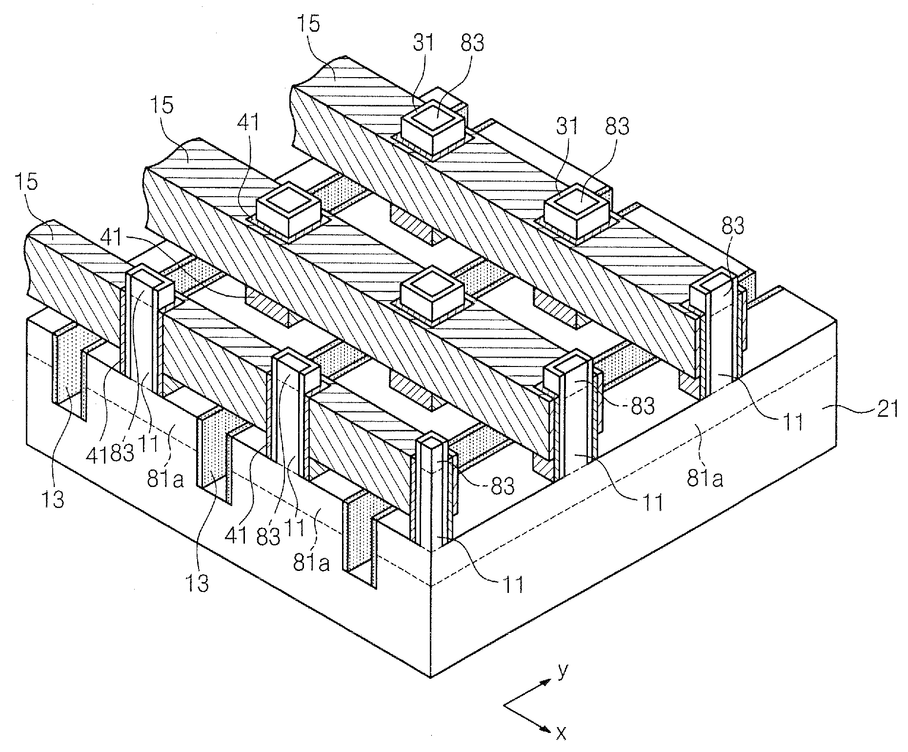
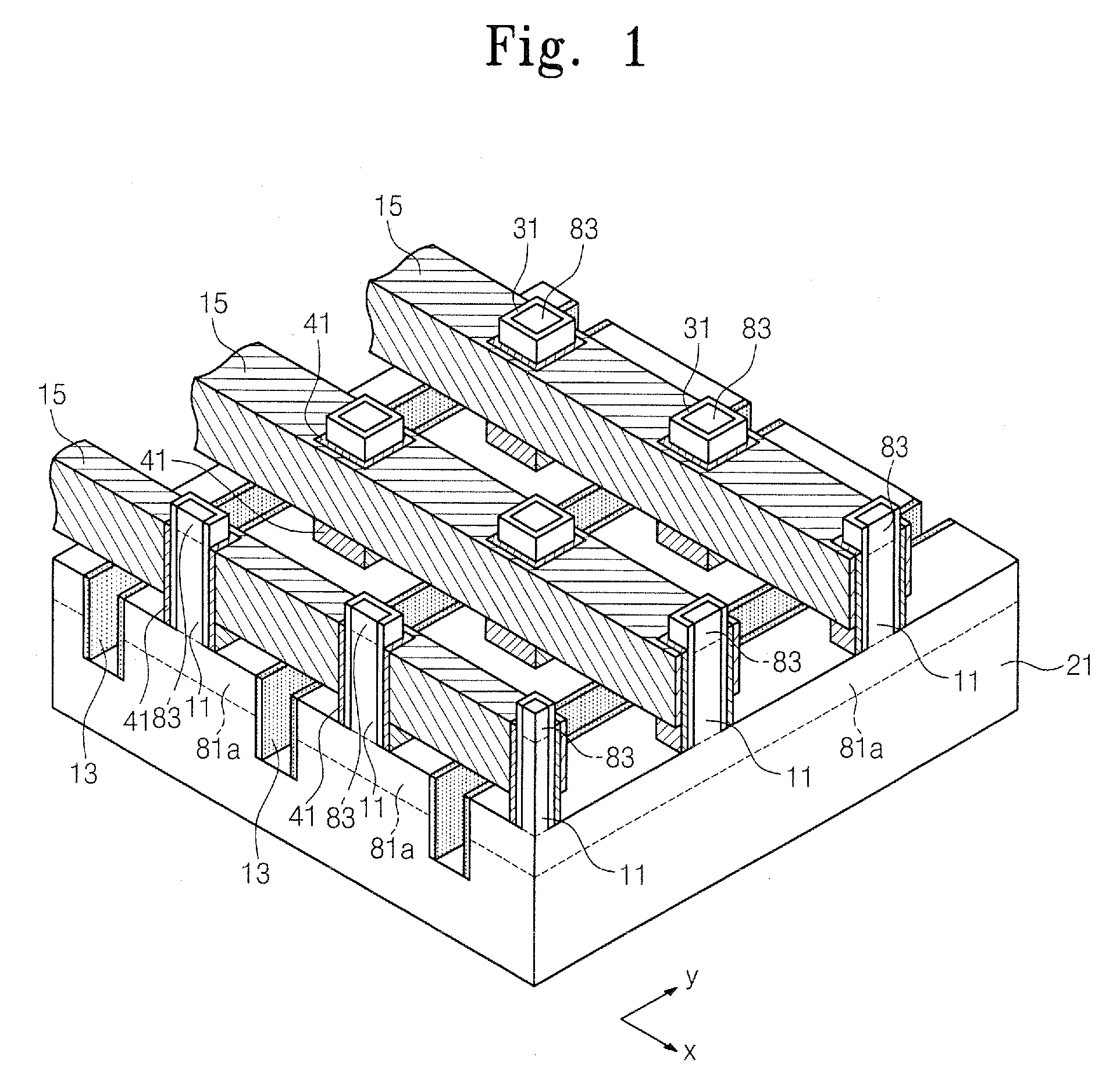
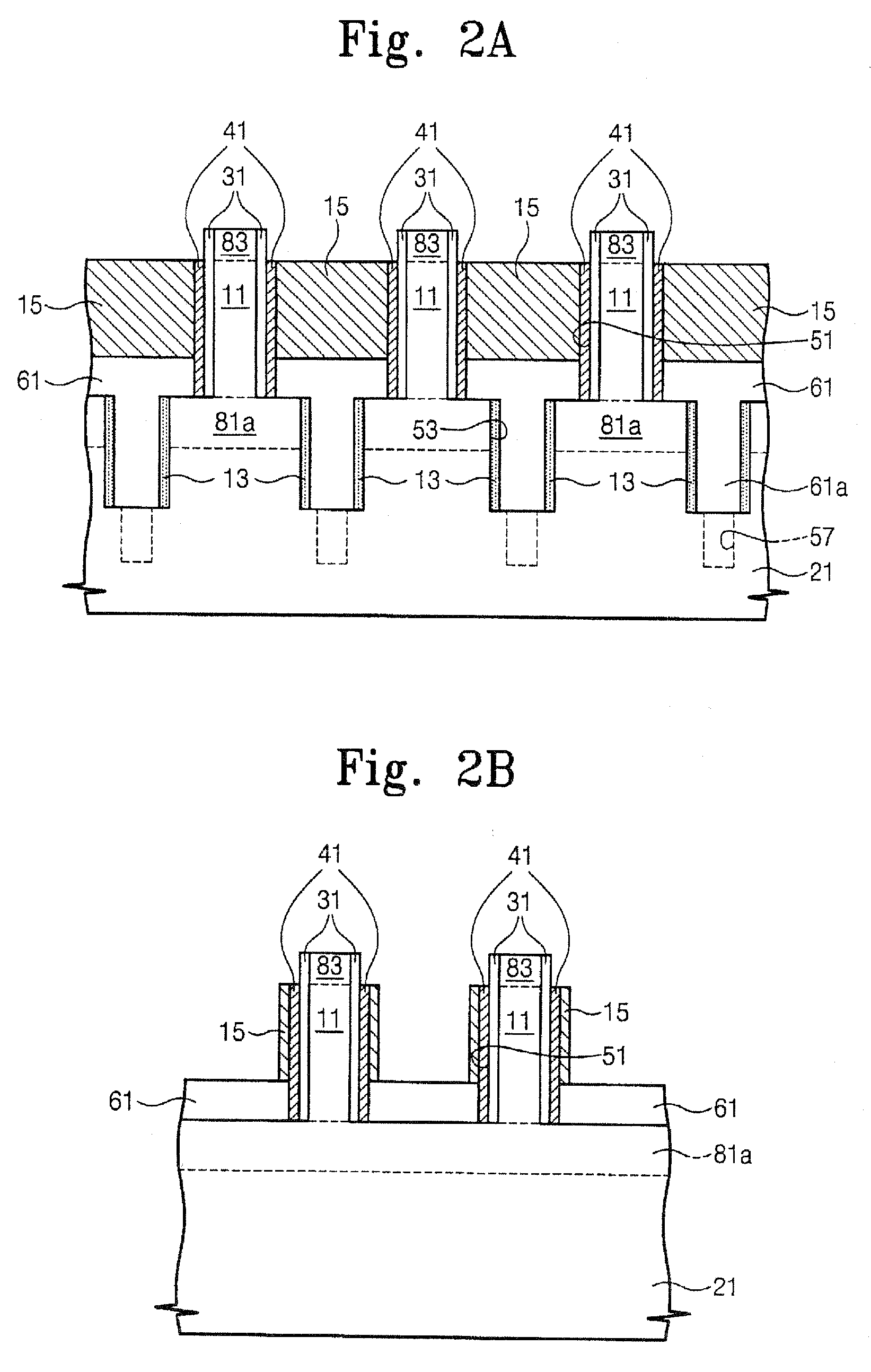
[0017]Exemplary embodiments of present invention will now be described more fully hereinafter with reference to the accompanying drawings. These exemplary embodiments may, however, be realized in many different forms and should not be construed as limited to the embodiments set forth herein. Rather, these embodiments are provided so that this disclosure will be thorough and complete, and will fully convey the scope of the invention to those skilled in the art.

[0018]It will be understood that when a material layer such as a conductive layer, a semiconductor layer or an insulation layer is referred to as being “on” another material layer or substrate, it can be directly on the other material layer or substrate or intervening layers may be present therebetween.

[0019]It will be understood that, although the terms fist, second, third, etc. may be used herein to describe various material layers or process steps, these layer or process steps should not be limited by these terms. These term...


PUM


Abstract

A method of forming a buried interconnection includes removing a semiconductor substrate to form a groove in the semiconductor substrate. A metal layer is formed on inner walls of the groove using an electroless deposition technique. A silicidation process is applied to the substrate having the metal layer, thereby forming a metal silicide layer on the inner walls of the groove.

Description

CROSS-REFERENCE TO RELATED APPLICATION[0001]This application claims the benefit of foreign priority to Korean Patent Application No. 10-2006-52073, filed Jun. 9, 2006, the disclosure of which is incorporated herein by reference in its entirety.BACKGROUND[0002]1. Field of Invention[0003]Embodiments of the present invention relate generally to methods of forming semiconductor devices including a buried interconnection line and, more particularly, to methods of forming semiconductor devices including a buried bit line.[0004]2. Description of the Related Art[0005]As semiconductor devices become more highly integrated, transistors included therein shrink in size. Shrinkage of the transistors leads to a reduction of active regions, in size, where the transistors are formed. Accordingly, the transistors of highly integrated semiconductor devices may suffer from a short channel effect and / or a narrow width effect.[0006]A three dimensional transistor such as a vertical transistor has been pr...

Claims


Application Information

Patent Timeline
Patent Type & Authority Applications(United States)
IPC IPC(8): H01L27/10H01L21/44
CPCH01L27/10885H01L27/10876H10B12/053H10B12/482H01L21/28H01L21/3205
Inventor YUN, JONG-HOKIM, BYUNG-HEEKIM, DAE-YONGKIM, HYUN-SUJUNG, EUN-JILEE, EUN-OK
Owner SAMSUNG ELECTRONICS CO LTD
Why Eureka
Try Eureka