
Monitoring pattern for detecting a defect in a semiconductor device and method for detecting a defect

Inactive Publication Date: 2007-12-27
SAMSUNG ELECTRONICS CO LTD
View PDF13 Cites 15 Cited by
  • Summary
  • Abstract
  • Description
  • Claims
  • Application Information

AI Technical Summary

Benefits of technology

[0012]The present invention is therefore directed to a monitoring pattern for detecting a defect in a semiconductor circu

Problems solved by technology

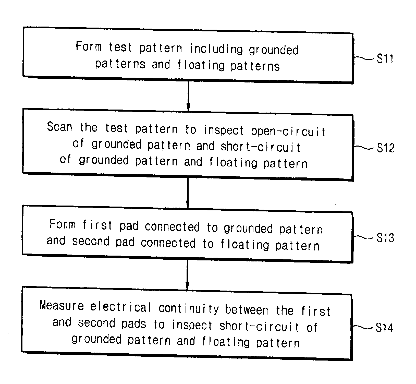
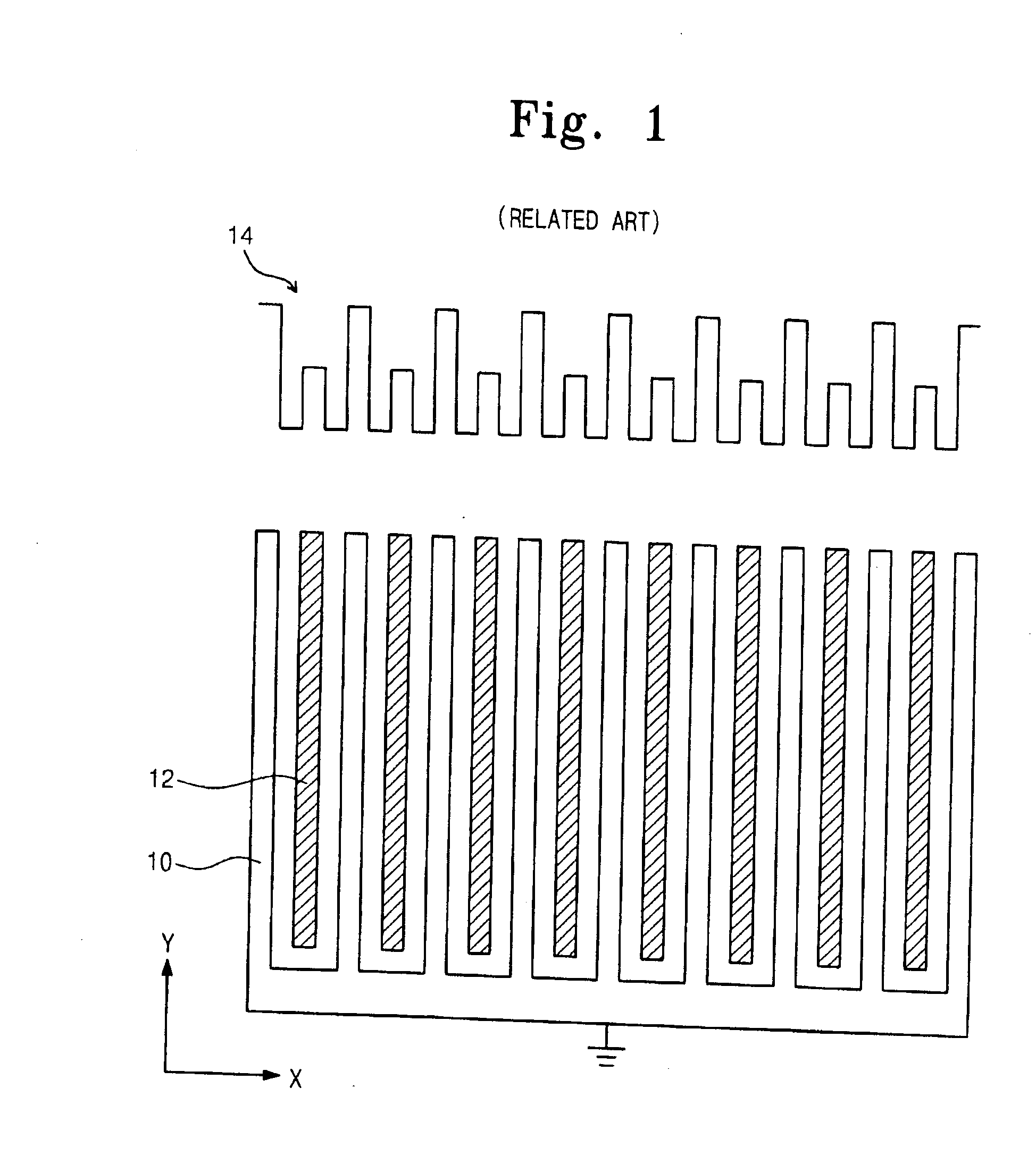
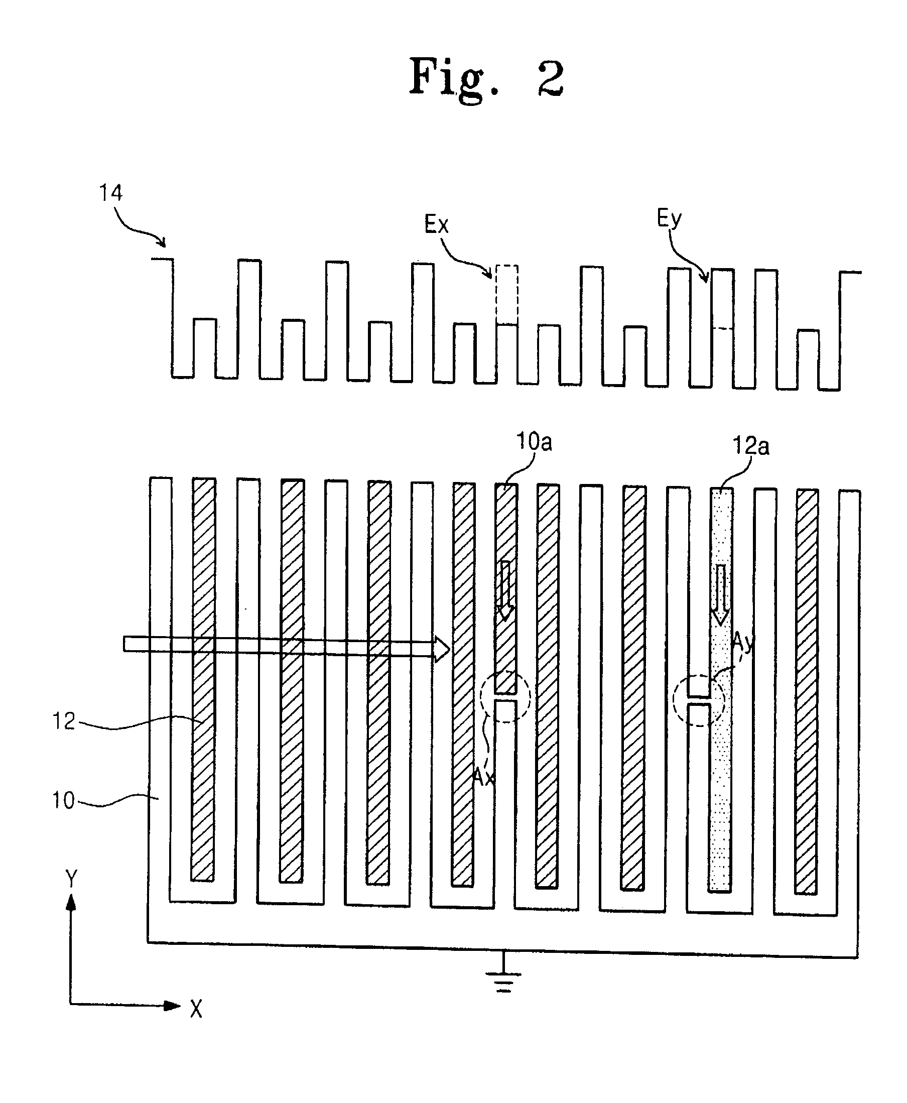
Nonetheless, the voltage contrast inspection may be incapable of judging whether the defect detected by the voltage contrast inspection is an electrical defect causing a malfunction of a semiconductor device.

Method used


Image

  • Monitoring pattern for detecting a defect in a semiconductor device and method for detecting a defect
  • Monitoring pattern for detecting a defect in a semiconductor device and method for detecting a defect
  • Monitoring pattern for detecting a defect in a semiconductor device and method for detecting a defect

Examples


first embodiment

[0029]FIG. 3 illustrates a monitoring pattern according to the present invention. The monitoring pattern may include a test pattern for a voltage contrast inspection. The test pattern may include a first pattern set including a grounded pattern 100 and a second pattern set including a floating pattern 102. The monitoring pattern may be designed so that line feature portions of the grounded pattern 100 and line feature portions of the floating pattern 102 are alternately arranged. The line feature portions of the grounded pattern 100 may be connected independently to a ground potential or connected in parallel thereto. On the other hand, the line feature portions of the grounded pattern 100 may be isolated from each other.

[0030]The monitoring pattern may be designed to employ the same layout as an existing test pattern for the voltage contrast inspection. Accordingly, during the voltage contrast inspection, defects in the test pattern may be detected by analyzing an intensity graph o...

second embodiment

[0036]FIG. 4 illustrates a monitoring pattern according to the present invention. In the monitoring pattern, a test pattern for a voltage contrast inspection may include a first pattern set including a line feature portion of a grounded pattern 200 and a second pattern set including a floating pattern 202. The grounded pattern 200 may be designed with a ladder shape to be connected to a ground potential. The floating pattern 202 may be a line-shaped pattern, which may be located between line feature portions of the grounded pattern 200. As a result, the grounded pattern 200 and the floating pattern 202 may have alternately arranged line feature portions.

[0037]The monitoring pattern further may include an interconnection layer for verifying an electrical continuity of the test pattern. A first interconnection 205a and a second interconnection 205b may be connected to the grounded pattern 200 and the floating pattern 202, respectively. The first interconnection 205a and the second int...

third embodiment

[0039]FIG. 5 illustrates a monitoring pattern according to the present invention. The monitoring pattern may include a test pattern for a voltage contrast inspection. The test pattern may be designed with a pattern set including multiple grounded patterns 300a and 300b.

[0040]Each of the grounded patterns 300a and 300b may take the shape of an “U” where both branches extend in one direction. The first grounded patterns 300a, where the branches extend in a first direction, may constitute a first sub-set. The second grounded patterns 300b, where the branches extend in a second direction, may constitute a second sub-set. One of the branches of the second grounded patterns 300b may extend between the branches of the first grounded patterns 300a. One of the branches of the first grounded patterns 300a may extend between the branches of the second grounded patterns 300b. In a line feature portion of the test pattern, the first and second grounded patterns 300a and 300b may be designed to ...


PUM


Abstract

A monitoring pattern for detecting a defect in a semiconductor device allows a voltage contrast inspection which may be verified by an electrical test where no special test pattern is required for the electrical test. The monitoring pattern includes a test pattern with line shapes arranged in parallel and spaced apart at predetermined linewidths and intervals, and an interconnection layer connected to the test pattern, where the test pattern is adapted to be charged with a specific potential to be displayed as a voltage contrast image when scanned with an electron beam.

Description

BACKGROUND OF THE INVENTION[0001]1. Field of the Invention[0002]The present invention relates to monitoring patterns for detecting a defect in a semiconductor circuit and methods for detecting the defect. More particularly, the present invention relates to monitoring patterns for detecting a defect by electron beam scanning and method for detecting the defect.[0003]2. Description of the Related Art[0004]Voltage contrast inspection has been used to monitor semiconductor circuits and processes. The voltage contrast inspection may utilize the intensity of secondary electrons, released when a test pattern is exposed to electron beam, which may be represented as a voltage contrast image.[0005]In a test pattern, a low potential state portion may be a high intensity portion of secondary electrons, while a high potential state portion may be a low intensity portion thereof. The low potential state portion may thus be brightly displayed, while the high potential state portion may be darkly d...

Claims


Application Information

Patent Timeline
IPC IPC(8): G01R31/26
CPCG01R31/307G01R31/2884H01L21/67288H01L22/12
Inventor BAE, CHOEL-HWYIHAN, YONG-WOONLEE, MI-JOUNGKWON, SANG-DEOK
Owner SAMSUNG ELECTRONICS CO LTD
Learn More