Low-power SRAM memory cell

a memory cell, low-power technology, applied in the direction of information storage, static storage, digital storage, etc., can solve the problems of large power consumption, large power waste, instability of the memory cell, etc., and achieve the effect of consumption of a relatively small amount of power

Active Publication Date: 2007-12-27
NAT TAIWAN UNIV
View PDF8 Cites 113 Cited by
  • Summary
  • Abstract
  • Description
  • Claims
  • Application Information

AI Technical Summary

Benefits of technology

[0016] Therefore, the object of the present invention is to provide an SRAM memory cell that consumes a relatively small amount of power when writing a write value of ‘0’ to the memory cell.

Problems solved by technology

As a result, a substantial amount of power is wasted.
In this instance, a full voltage swing occurs to ensure the required logic states at the nodes (D1, D2), which results in substantial power consumption.
The proposed scheme, however, results in instability of the memory cell.

Method used


Image

  • Low-power SRAM memory cell
  • Low-power SRAM memory cell
  • Low-power SRAM memory cell

Examples


Embodiment Construction

[0047] Before the present invention is described in greater detail, it should be noted that like elements are denoted by the same reference numerals throughout the disclosure.

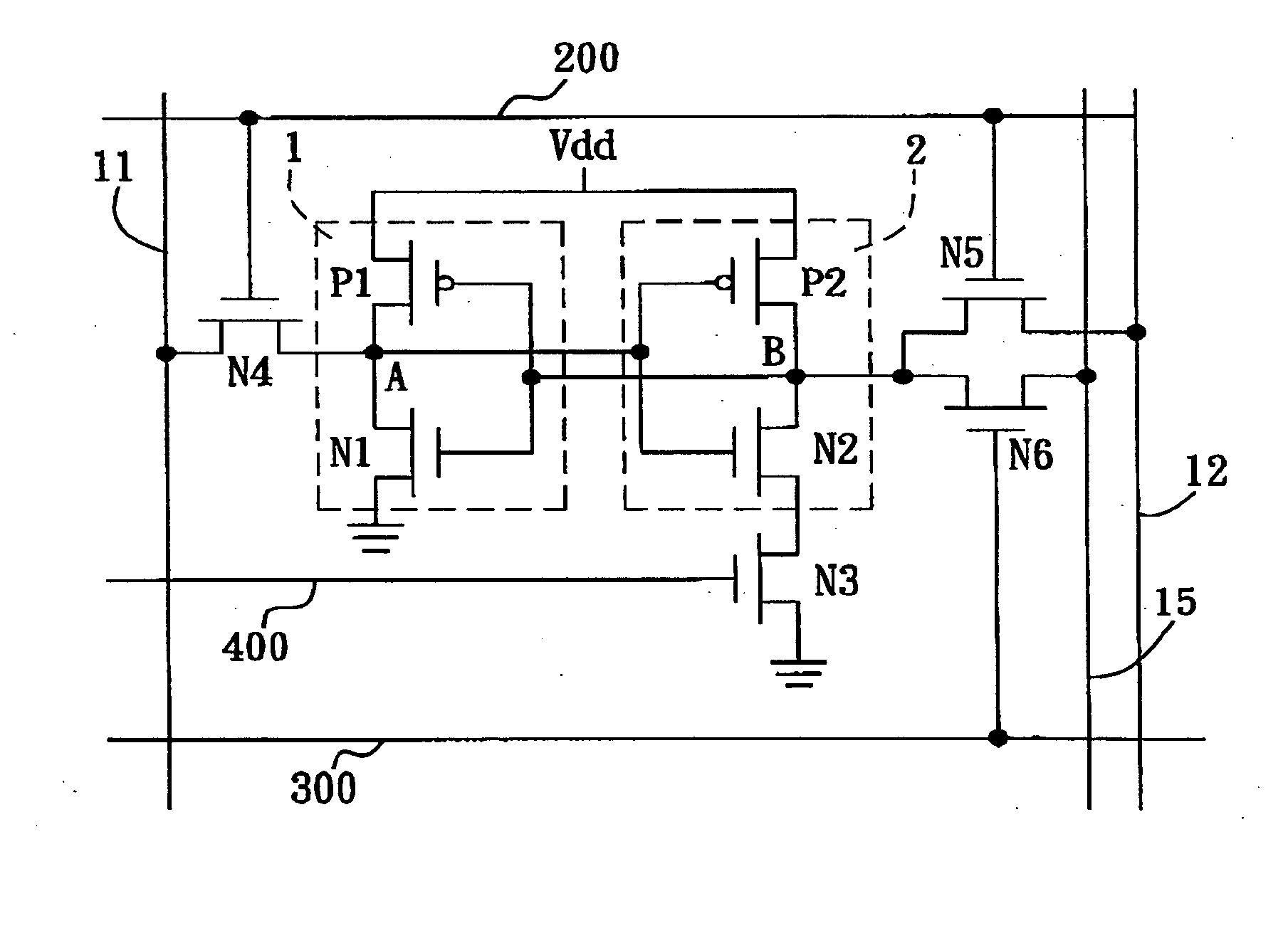
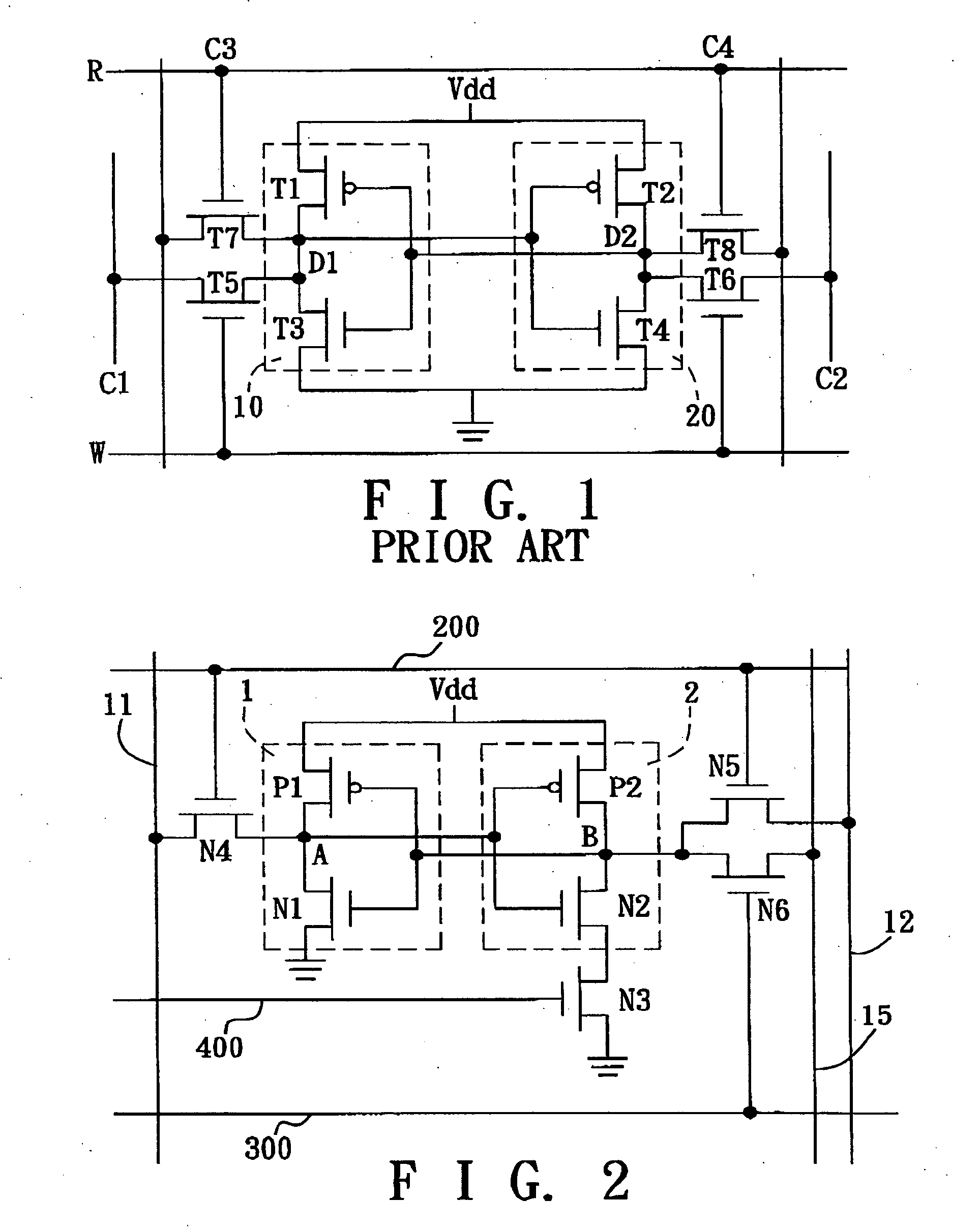
[0048] Referring to FIG. 2, the first preferred embodiment of a low-power SRAM memory cell according to this invention is shown to comprise a first inverter 1, a second inverter 2, a switching transistor (N3), two read access transistors (N4, N5), and a write access transistor (N6).

[0049] The first inverter 1 includes a pair of transistors (P1, N1) that are coupled in series. The second inverter 2 likewise includes a pair of transistors (P2, N2) that are coupled in series. The transistors (P1, P2) are PMOS field effect transistors, whereas the transistors (N1, N2) are NMOS field effect transistors. The first and second inverters 1, 2 are cross-coupled. That is, the transistors (P2, N2) of the second inverter 2 have gate terminals that are coupled to a common connection node (A) of the transistors (P1, N1) of ...


PUM


Abstract

An SRAM memory cell that has a relatively small power consumption when writing a write value of ‘0’ to the memory cell includes cross-coupled first and second inverters, at least one read access transistor for selectively coupling a respective read bit line to a common connection node of a respective one of the first and second inverters, a switching transistor for selectively coupling the second inverter to a ground terminal, and a write access transistor for selectively coupling the common connection node of the second inverter to a write bit line.

Description

CROSS-REFERENCE TO RELATED APPLICATIONS [0001] This application claims priority of Taiwanese application no. 092126407, filed on Sep. 24, 2003, and U.S. provisional patent application No. 60 / 603,980, filed on Aug. 24, 2004.BACKGROUND OF THE INVENTION [0002] 1. Field of the Invention [0003] The invention relates to a semiconductor memory cell, more particularly to an SRAM memory cell that consumes a relatively small amount of power when writing a write value of ‘0’ to the memory cell. [0004] 2. Description of the Related Art [0005] Random access memories (RAM) can be classified into dynamic random access memories (DRAM) and static random access memories (SRAM), the latter being commonly employed in cache memories in view of their fast access times. [0006]FIG. 1 illustrates a conventional SRAM memory cell that has a write port and a read port, and that is formed from eight transistors (T1-T8). The transistors (T1, T2) are PMOS field effect transistors, whereas the transistors (T3, T4)...

Claims


Application Information

Patent Timeline
Patent Type & Authority Applications(United States)
IPC IPC(8): G11C7/12
CPCG11C11/413G11C11/412
Inventor CHANG, YEN-JENLAI, FEIPEIYANG, CHIA-LIN
Owner NAT TAIWAN UNIV
Why Eureka
Try Eureka