Flip-chip package structure with stiffener

a package structure and flip-chip technology, applied in the direction of electrical equipment, semiconductor devices, semiconductor/solid-state device details, etc., can solve the problems of substrate bending, difficult control of manufacturing process problems, adverse effects on etc., to achieve good cleaning effect of flux, improve the coplanarity of the flip-chip package structure during reflow, and simple flip-chip package structure and a method

Active Publication Date: 2008-01-03
ADVANCED SEMICON ENG INC
View PDF9 Cites 30 Cited by
  • Summary
  • Abstract
  • Description
  • Claims
  • Application Information

AI Technical Summary

Benefits of technology

[0018]According to the flip-chip package structure with stiffener and the method for manufacturing the same, a simple flip-chip package structure and a method are provided. Since the first stiffener is positioned on the substrate before connecting the chip to the substrate, the coplanarity of the flip-chip package structure during reflow is improved and, at the same time, the cleaning effect of the flux is kept good. Therefore the underfill can completely contact with the solder bumps and the substrate during the underfill dispensing process, and thus improves the package structure. The two-stage positioned second stiffener further improves the coplanarity of the flip-chip package structure.
[0019]Therefore the problems in the conventional manufacturing method are solved and the coplanarity of the flip-chip package structure is efficiently improved.

Problems solved by technology

However, due to the different coefficients of thermal expansion (CTE) between the chip and the substrate, the large-scaled flip-chip package structure is apt to bend during thermal treatment processes such as reflow process or curing process, and accordingly the coplanarity of the flip-chip package structure is adversely effected.
In addition, such problem is not easily controlled during manufacturing process, especially in the manufacturing process of the flip-chip package structure.
Therefore the problem of unfavorable coplanarity of the large-scaled flip-chip package structure is a problem that is in need of an immediate solution.
Such processes improve the cleaning effect of the flux but still suffers from substrate bending after positioning the chip on the substrate.
In other words, designing and positioning of the stiffener in the conventional manufacturing process of the flip-chip package structure still has an unsolved problem: it can not simultaneously improve the coplanarity of the flip-chip package structure and the cleaning effect of the flux, which is contributive to make the underfill completely contact with the solder bumps, the chip, and the substrate in order to protect the chip.

Method used


Image

  • Flip-chip package structure with stiffener
  • Flip-chip package structure with stiffener
  • Flip-chip package structure with stiffener

Examples


Embodiment Construction

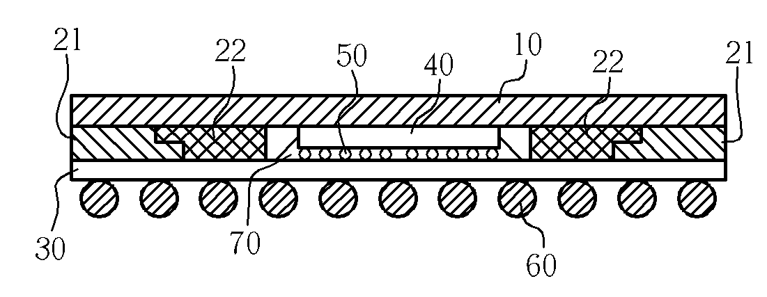
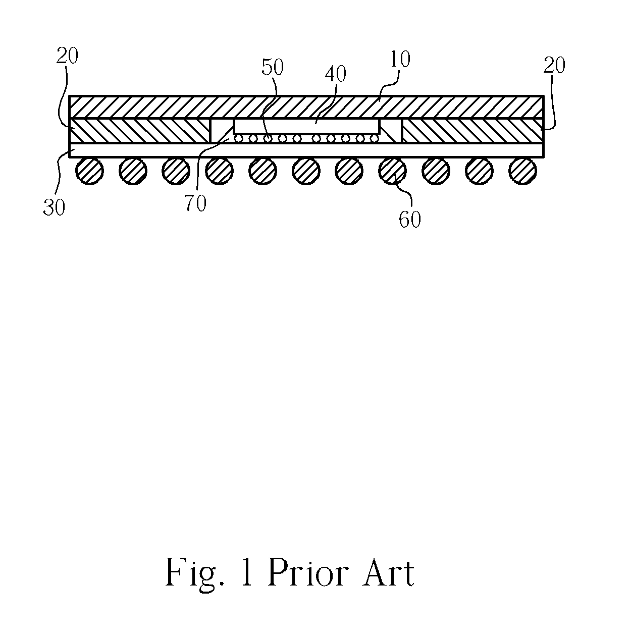
[0026]Please refer to FIG. 3, which is a schematic drawing of a flip-chip package structure provided by the present invention. The flip-chip package structure comprises a substrate 30, such as a circuit board, a first stiffener 21, which has an upper surface and a bottom surface larger than the upper surface, positioned on a surface of the substrate 30 with its bottom surface, a plurality of solder bumps 50, such as solder balls, for electrically connecting a chip 40 to the substrate 30, and an underfill 70 formed in between the substrate 30 and the chip 40 and encapsulating the solder bumps 50.

[0027]The flip-chip package structure provided by the present invention also comprises a second stiffener 22 positioned on the surface of the substrate 30 and connected with the first stiffener 21. The first stiffener 21 is positioned outside of the second stiffener 22. The first stiffener 21 and the second stiffener 22 can be ring-shaped. Junction parts of the first stiffener 21 and the seco...


PUM


Abstract

A flip-chip package structure with stiffener includes a substrate, a first stiffener positioned on a surface of the substrate, a chip having a plurality of bumps adopted to electrically connect the substrate and the chip, and a second stiffener positioned on the surface of the substrate and connected with the first stiffener. The first stiffener is positioned outside of the second stiffener.

Description

BACKGROUND OF THE INVENTION[0001]1. Field of the Invention[0002]The invention relates to a flip-chip package structure and a method for manufacturing the same, and more particularly, to a flip-chip package structure with stiffeners and a method for manufacturing the same.[0003]2. Description of the Prior Art[0004]Following the ever-present demand for decreasing the sizes and geometries of electronic components, the high-speed requirement and miniaturization in IC packaging technology are continually rising and become a principal objective of the IC packaging technology.[0005]The flip-chip package structure is therefore developed. Being different from traditional wire bonding packages, chips used in the flip chip package are inverted upside down on a substrate with solder bumps to provide electrical connection between the flip chip and the substrate. Thus the scales and the sizes of the package structures are efficiently decreased while its operation for high-speed signals and heat d...

Claims


Application Information

Patent Timeline
Patent Type & Authority Applications(United States)
IPC IPC(8): H01L23/48
CPCH01L23/16H01L23/3128H01L23/36H01L2224/73253H01L2924/15311H01L2224/16225H01L2924/16195H01L2224/32225H01L2224/73204H01L2924/00H01L2924/00011H01L2924/00014H01L2224/0401
Inventor CHEN, JAU-SHOUNG
Owner ADVANCED SEMICON ENG INC
Why Eureka
Try Eureka