High efficient phosphor-converted light emitting diode

a light-emitting diode, high-efficiency technology, applied in the direction of semiconductor/solid-state device manufacturing, semiconductor devices, electrical apparatus, etc., can solve the problem of achieve the effect of improving the overall light luminescence efficiency of the device and reducing the light luminescence efficiency loss

Active Publication Date: 2008-01-10
EPISTAR CORP
View PDF5 Cites 39 Cited by
  • Summary
  • Abstract
  • Description
  • Claims
  • Application Information

AI Technical Summary

Benefits of technology

[0006]This disclosure disclosed a light-emitting device and a method of forming the same. A phosphor layer is formed on the chip before encapsulation in order to avoid the disadvantage of above-mentioned known technology. Another purpose of the disclos

Problems solved by technology

Therefore, it can reduce the light luminescence efficiency loss caused by the absorption of the light which is back

Method used


Image

  • High efficient phosphor-converted light emitting diode
  • High efficient phosphor-converted light emitting diode
  • High efficient phosphor-converted light emitting diode

Examples


Embodiment Construction

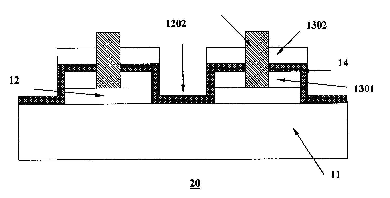
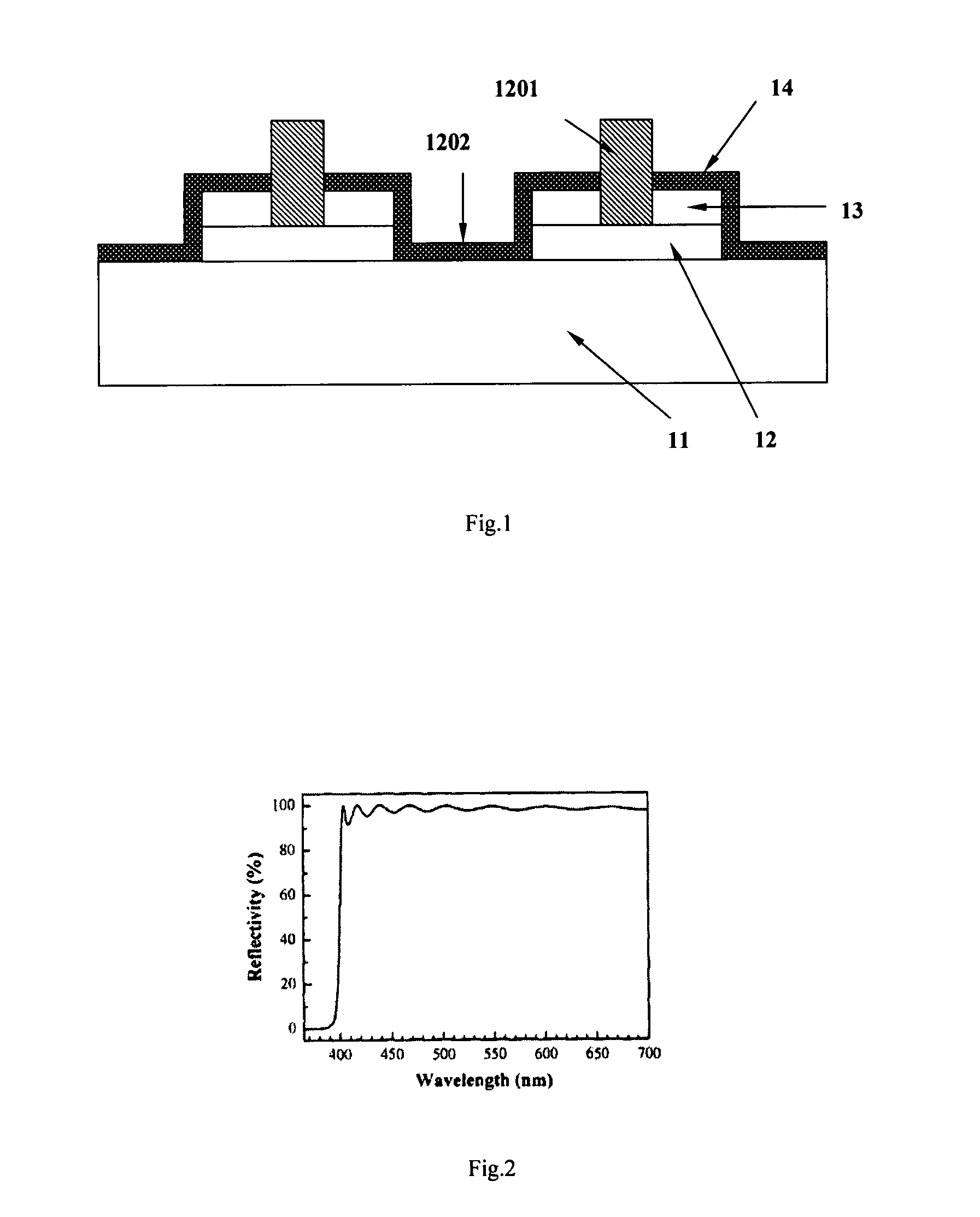
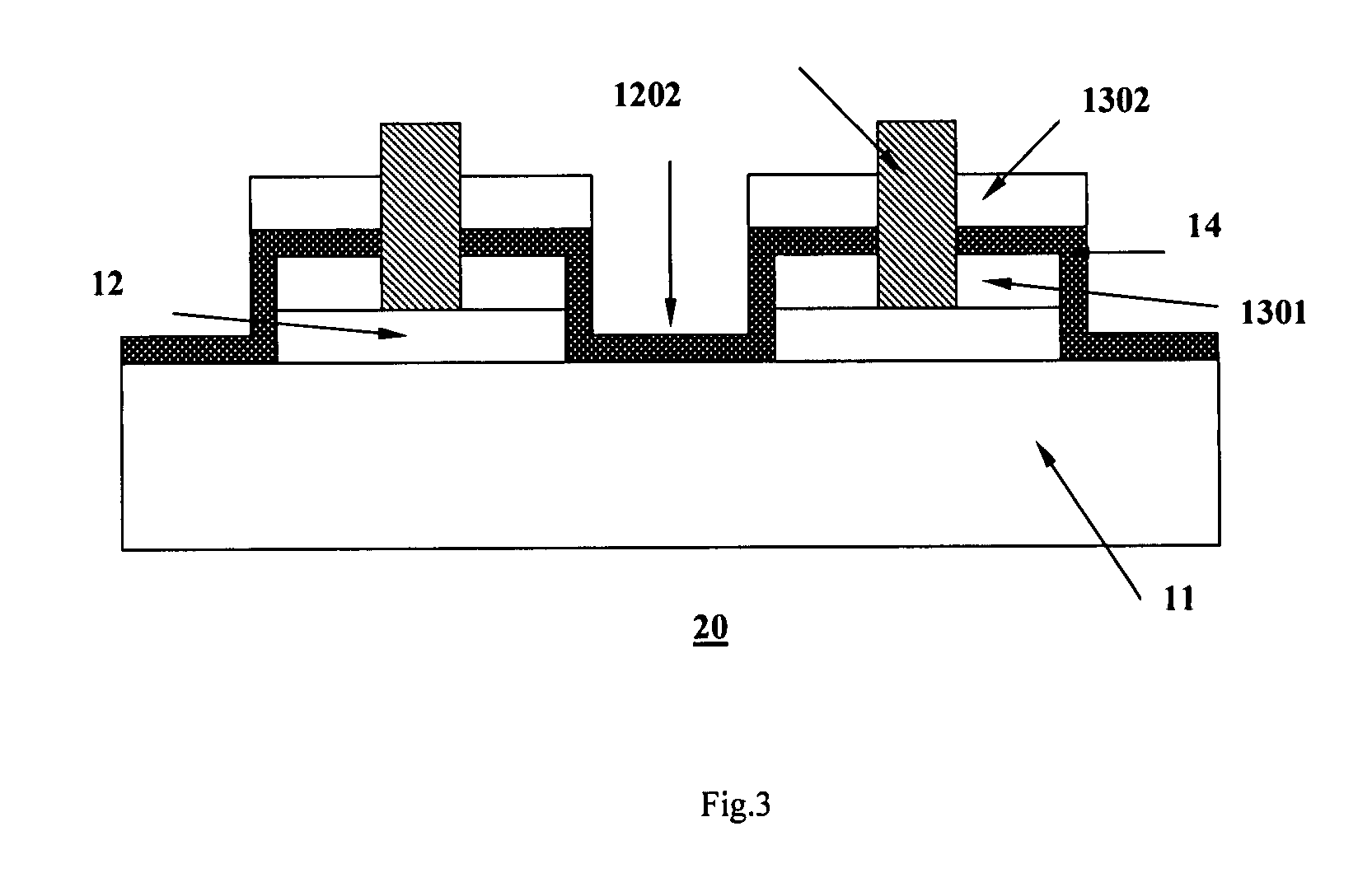
[0013]FIG. 1 shows a schematic view of the preferred embodiment of the present disclosure. The disclosure discloses a light-emitting device 10 comprising a substrate 11, a semiconductor layer 12 having an active layer to emit a first wavelength light, a filter layer 13 and a fluorescent conversion layer 14. The material of the substrate 11 is composed of either opaque material or transparent material. For opaque material, it can be semiconductors metal or other opaque materials. In a preferred embodiment, the material of the substrate is selected from the group of Si, GaN / Si, GaAs and the combination of the above materials. For transparent materials, it can be glass, sapphire, SiC, GaP, GaAsP, ZnSe, ZnS or ZnSSe. The structure of the semiconductor structure 12 is either vertical (the electrical contacts located on the different side of the structure) or horizontal (the electrical contacts located on the same side of the structure). When the first wavelength light passes the filter l...


PUM


Abstract

A light-emitting device and manufacturing method thereof are disclosed. The light-emitting device includes a substrate, a semiconductor light-emitting structure, a filter layer, and a fluorescent conversion layer. The method comprises forming a semiconductor light-emitting structure over a substrate, forming a filter layer over the semiconductor light-emitting structure, and forming a fluorescent conversion layer over the filter layer.

Description

CROSS REFERENCE TO RELATED APPLICATIONS[0001]This application claims the right of priority based on Taiwan Patent Application No. 095124433 entitled “High Efficient Phosphor-Converted Light Emitting Diode”, filed on Jul. 5, 2006, which is incorporated herein by reference and assigned to the assignee herein.TECHNICAL FIELD[0002]This present disclosure relates to a light-emitting device and a method of forming the same, especially has a filter layer and a fluorescent conversion layer.BACKGROUND OF THE DISCLOSURE[0003]The white light LED (Light-emitting diode, LED) technology can be divided into single-chip type and multiple-chips type. The multiple-chips type using LEDs of three colors to mix the light emitted respectively into the white light. The benefit of the multiple-chips type is the flexibility of the light mixing based on different visual demand. However, the cost is relatively high for using many of LEDs chips at the same time. Furthermore, because the materials of making the...

Claims


Application Information

Patent Timeline
IPC IPC(8): H01L29/06
CPCH01L33/50H01L33/44
Inventor WANG, CHIEN-YUANLU, CHIH-CHIANGHSIEH, MIN-HSUN
Owner EPISTAR CORP
Why Eureka
Try Eureka