Compound of nanostructures and polymer for use in electroluminescent device

a technology of nanostructures and polymers, applied in the field of materials, can solve the problems of deterioration of organic el devices, change in the properties of organic luminous layers, and prolonging the useful life of el devices

Inactive Publication Date: 2008-01-10
YAZAKI CORP
View PDF5 Cites 28 Cited by
  • Summary
  • Abstract
  • Description
  • Claims
  • Application Information

AI Technical Summary

Problems solved by technology

However, because some of the recombining of holes and electrons actually takes place outside of the luminous layer, many of the carriers are converted into thermal vibrations or energy other than visible light.
The main causes of deterioration in an organic EL device are penetration into, and attachment to, the organic luminous layer by active molecules of water and changes in the properties of the organic luminous layer.
Second, doping carbon nanostructures into the

Method used


Image

  • Compound of nanostructures and polymer for use in electroluminescent device
  • Compound of nanostructures and polymer for use in electroluminescent device
  • Compound of nanostructures and polymer for use in electroluminescent device

Examples


Embodiment Construction

[0027]It is to be understood by one of ordinary skill in the art that the present discussion is a description of exemplary embodiments only, and is not intended as limiting the broader aspects of the present invention, which broader aspects are embodied in the exemplary construction.

Light Emitting Compound

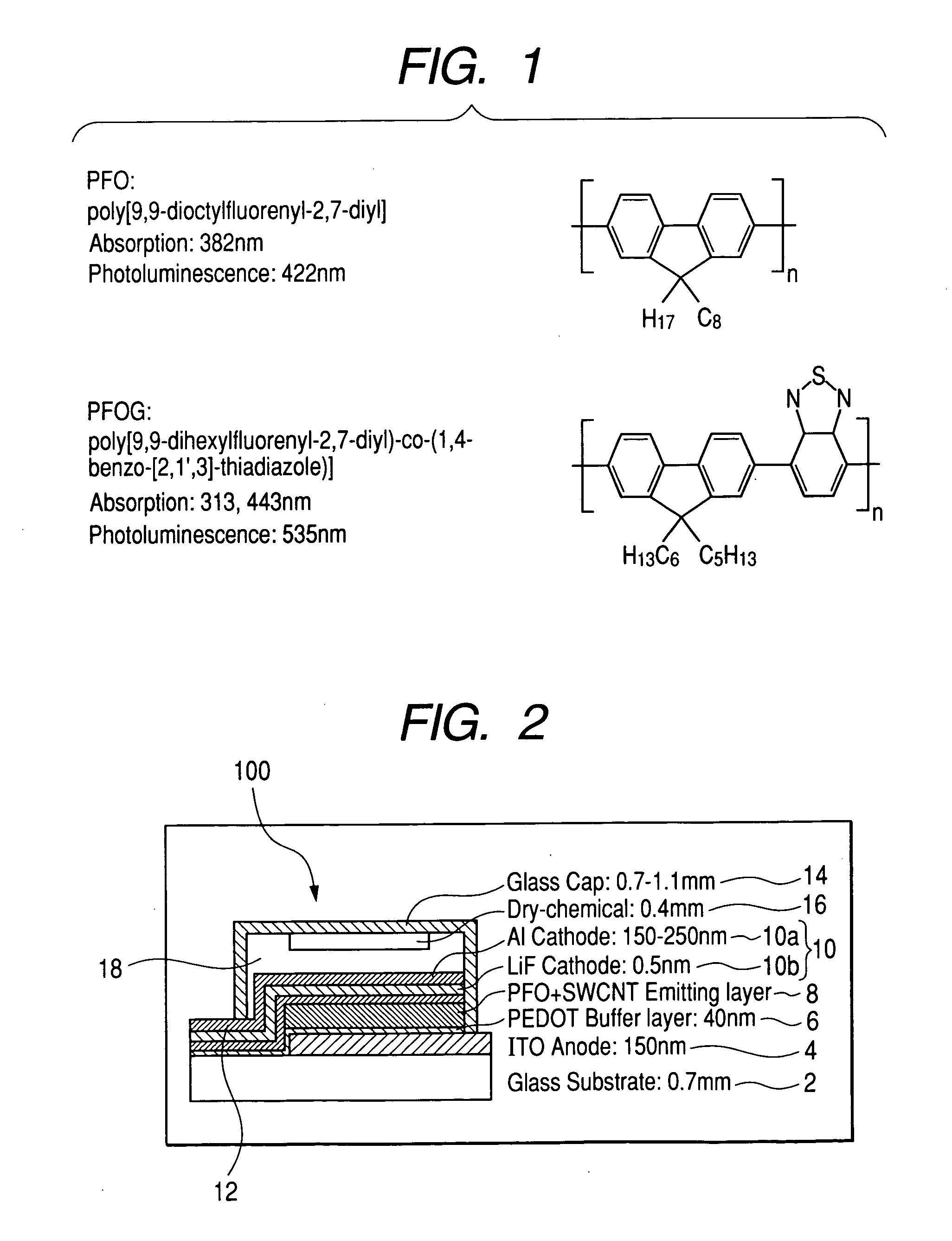
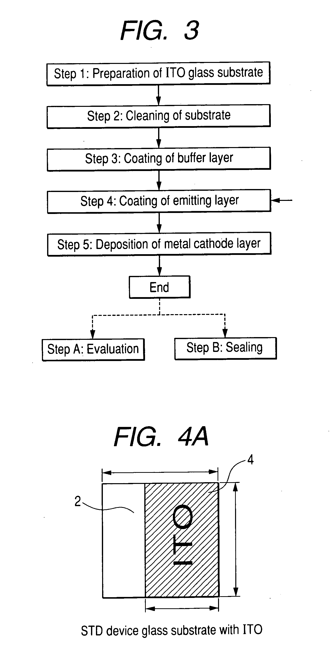
[0028]A light emitting material according to an exemplary embodiment of the invention is a compound of a polyfluorene (PFO) polymer host material doped with nanostructures. The compound can be used as an emitting layer of an EL device.

[0029]Examples of PFO polymers suitable for use as the host material are PFOG, PFOR, and PFOB. Specifically, PFO: poly[9,9-diocytlfluorenyl-2,7-diyl], which has an absorption of 382 nm and a photoluminescence at 422 nm and PFOG: poly[9,9-dihexylfluorenyl-2,7-diyl]-co-(1,4,-benzo-[2,1′,3]-thadizole)], which has an absorption of 313 nm or 443 nm and a photoluminescence at 535 nm, are suitable structures. However, the invention is not limited in this res...


PUM

PropertyMeasurementUnit
Lengthaaaaaaaaaa
Fractionaaaaaaaaaa
Percent by massaaaaaaaaaa

Abstract

A compound for use in an electroluminescent device, including 0.001% to 10% by weight of nanostructure and a polyfluorene polymer. The compound can be used as a light emitting layer of an EL device including a cathode, an anode, and the light emitting layer disposed between the cathode and the anode. The EL device can be manufactured by providing a substrate, providing an anode or cathode on the substrate, and depositing the emitting layer on the substrate. The compound can be manufactured by ultrasonically cutting nanostructures and mixing the nanostructures with a polymer, such as the polyfluorene polymer.

Description

FIELD OF THE INVENTION[0001]The present invention relates to electroluminescent (EL) devices, such as self-light-emitting elements. More particularly, the present invention relates to the materials used in EL devices.BACKGROUND OF THE INVENTION[0002]EL devices can be used as light sources for flat-type self-light-emitting display devices for purposes. For example, flat-type self-light-emitting elements can be used in automotive instrument display panels. In general, an EL device is a spontaneously luminous element characterized by injecting electrons and electron holes (i.e., carriers) into an inorganic or organic layer provided between electrodes, and recombining the electrons and electron holes in a luminous layer. Light is produced when the electrons and electron holes recombine.[0003]Although EL devices have achieved some practical use, there is room for improvement with respect to driving voltage requirements, useful life, brightness or luminous efficiency, and manufacturing te...

Claims


Application Information

Patent Timeline
IPC IPC(8): H01L51/54H01L51/56H01B1/00H01B1/24
CPCB82Y10/00C09K11/06C09K2211/1416C09K2211/1483H01L51/0039Y10T428/2918H01L51/5036H05B33/14Y10T428/25Y10T428/2975H01L51/0048H10K85/115H10K85/221H10K50/125
Inventor CARROLL, DAVID L.HOSHI, SAKUTARO
Owner YAZAKI CORP
Why Eureka
Try Eureka