Memory elements using organic active layer

a technology of active layer and memory element, applied in thermoelectric devices, instruments, nanoinformatics, etc., can solve the problems of volatile memory devices losing their information, slowing down faster than other types of storage devices, and increasing the volume, use and complexity of computers and electronic devices

Active Publication Date: 2006-09-05
SPANSION LLC +1
View PDF12 Cites 6 Cited by
  • Summary
  • Abstract
  • Description
  • Claims
  • Application Information

AI Technical Summary

Problems solved by technology

The volume, use and complexity of computers and electronic devices are continually increasing.
The long term storage mediums typically store larger amounts of information at a lower cost, but are slower than other types of storage devices.
Volatile memory devices generally lose their information if they lose power and typically require periodic refresh cycles to maintain their information.
However, silicon-based devices are approaching their fundamental physical size limits.
Inorganic solid state devices are generally encumbered with a complex architecture which leads to high cost and a loss of data storage density.
The volatile semiconductor memories based on inorganic semiconductor material must constantly be supplied with electric current with a resulting heating and high electric power consumption in order to maintain stored information.
Non-volatile semicon...

Method used


Image

  • Memory elements using organic active layer
  • Memory elements using organic active layer
  • Memory elements using organic active layer

Examples


first embodiment

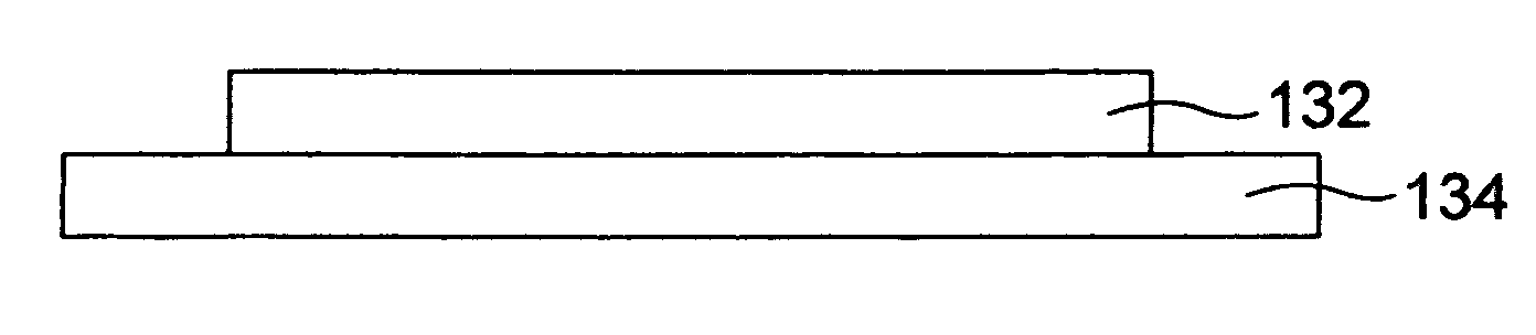
[0031]FIGS. 7–10 illustrate a process for fabricating memory element 130 in accordance with the present invention. Initially, an electrode 132 is formed on a substrate 134 (FIG. 7). The electrode 132 may be formed by any suitable technique, such as physical vapor deposition, i.e. PVD (such as thermal vacuum evaporation, e-beam deposition or sputtering), ion plating, chemical vapor deposition, i.e. CVD (such as metal-organic CVD, i.e. MOCVD), plasma-enhanced CVD, i.e. PECVD, and the like. The electrode 132 in this embodiment is copper, but it will be understood that the electrode 132 can be formed of any of a number of materials including aluminum, barium, calcium, chromium, cobalt, copper, germanium, gold, magnesium, manganese, molybdenum, indium, iron, nickel, palladium, platinum, ruthenium, samarium, silver, tantalum, titanium, tungsten, zinc, metal oxides, polysilicon, doped amorphous silicon, metal silicide, metal carbide, metal nitrides, magnesium-silver alloy, nickel-cobalt al...

second embodiment

[0044]FIG. 12 illustrates memory element 230. In this embodiment, again, an electrode 232 of, for example, copper is provided on, over and in contact with a substrate 234, a passive layer 236, for example, copper sulfide is provided on, over in contact with the electrode 232, an active layer 238 (approximately 700 angstroms thick) in the form of a polyfluorene layer is provided on, over and in contact with the passive layer 236, and an electrode 240 of, for example, titanium, is provided on, over and in contact with the polyfluorene layer 238, with the active and passive layers 238, 236 between the electrodes 232, 240. The memory element 230 takes the form of and is fabricated in the same manner as the memory element 130, described above. Again, arylenes can include heterocycles such as pyridine, bipyridine, quinoline, biquinoline, tepyridine, thiophene, bithiophene, and alkyl- or alkoxy-substituted derivatives thereof, which provide with the polyfluorene copolymer a polyfluorene he...


PUM

PropertyMeasurementUnit
Chemical structureaaaaaaaaaa

Abstract

A memory element includes a first electrode, a passive layer on and in contact with the first electrode, a polyfluorene active layer on and in contact with the active layer, and a second electrode on and in contact with the polyfluorene active layer. The chemical structure of the polyfluorene active layer may be altered to take different forms, each providing a different memory element operating characteristic.

Description

BACKGROUND OF THE INVENTION[0001]1. Technical Field[0002]This invention relates generally to memory devices, and more particularly, to memory element fabrication and configuration.[0003]2. Background Art[0004]The volume, use and complexity of computers and electronic devices are continually increasing. Computers consistently become more powerful, new and improved electronic devices are continually developed (e.g., digital audio players, video players). Additionally, the growth and use of digital media (e.g., digital audio, video, images, and the like) have further pushed development of these devices. Such growth and development has vastly increased the amount of information desired / required to be stored and maintained for computer and electronic devices.[0005]Generally, information is stored and maintained in one or more of a number of types of storage devices. Storage devices include long term storage mediums such as, for example, hard disk drives, compact disk drives and correspon...

Claims


Application Information

Patent Timeline
IPC IPC(8): H01L35/24H01L51/00
CPCB82Y10/00G11C13/0014G11C13/0016H01L27/285H01L51/0043H01L51/0036H01L51/0039H10K19/202H10K85/115H10K85/113H10K85/151
Inventor KINGSBOROUGH, RICHARDSOKOLIK, IGORGAUN, DAVIDKAZA, SWAROOPPANGRLE, SUZETTENICKEL, ALEXANDERSPITZER, STUART
Owner SPANSION LLC
Why Eureka
Try Eureka