Testing method and testing device for an integrated circuit

Active Publication Date: 2008-01-10
ROBERT BOSCH GMBH
View PDF10 Cites 0 Cited by
  • Summary
  • Abstract
  • Description
  • Claims
  • Application Information

AI Technical Summary

Benefits of technology

[0005] The testing method according to the present invention advantageously exhibits increased stability and, compared with the related art, greater independence from hardware-related loads. Moreover, the testing method is more independent from chip-internal states (e.g., charged circuit nodes) and external effects.

Problems solved by technology

A disadvantage of this testing method is that the resulting characteristic curve is barely dependent on the structure of the integrated circuit.
It has been found in experiments that this testing method is therefore unsuitable for detecting certain crystal defects and aluminum spiking.
Therefore, it may be the case that certain defective integrated circuits enter the market, which represents a safety risk in particular in safety-relevant vehicle electronics.

Method used


Image

  • Testing method and testing device for an integrated circuit
  • Testing method and testing device for an integrated circuit

Examples


Embodiment Construction

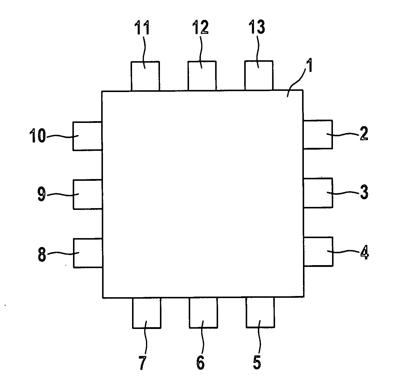
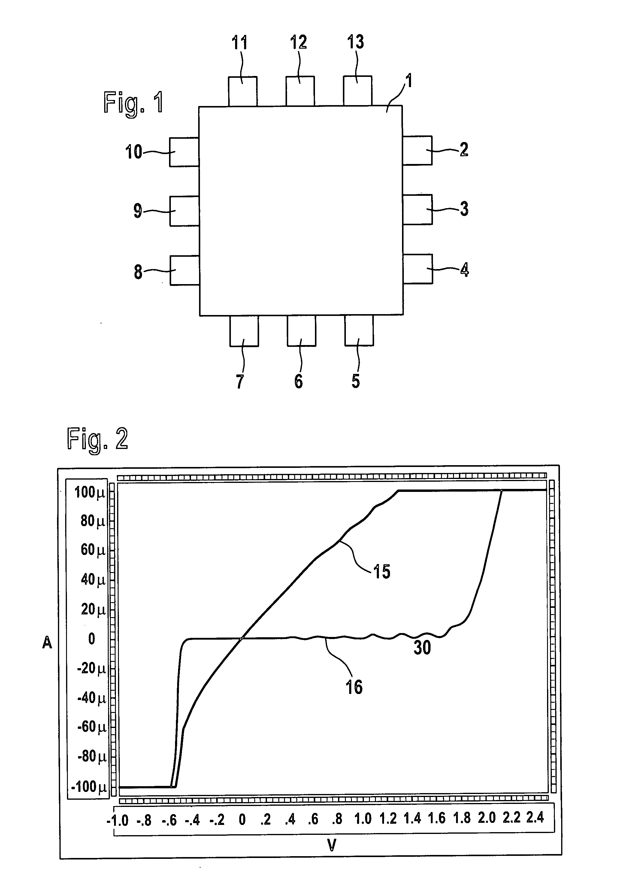
[0014]FIG. 1 shows a schematic view of an integrated circuit 1 which is typically an ASIC (application-specific integrated circuit). The integrated circuit has multiple electrical terminals 2 through 13. These terminals are internally connected to components such as diodes, bipolar transistors, field-effect transistors, resistors, and capacitors. Internal connections via integrated components exist between terminals 2 through 13.

[0015] For testing the functionality, a ground potential (grounding) is applied to each of ground terminals 2, 3 and another variable potential is applied to signal terminal 4. No potential (floating potential) is applied to further signal terminals 5 through 13. For example, between ground terminals 2 and 3 and signal terminal 4 an internal connection exists via one or multiple integrated components or a pn junction (diode) is formed such as, for example, between the substrate and the source or the drain of a field-effect transistor. For testing the functi...


PUM


Abstract

A testing method for an integrated circuit which has at least one ground terminal and multiple signal terminals, a signal potential being applied to a signal terminal and a ground potential being applied to the at least one ground terminal. A floating potential is applied to each further signal terminal. The testing method is suitable to detect more defects than a standard testing method of the Automotive Electronics Council.

Description

BACKGROUND INFORMATION [0001] In a testing method, which is recognized by the Automotive Electronics Council as the standard in quality assurance, for an integrated circuit which has at least one ground terminal and multiple signal terminals a signal potential is applied to one signal terminal and a ground potential (grounding) is applied to the at least one ground terminal. A ground potential is applied to all other signal terminals. Signal terminal in this connection means each terminal which is not intended to be connected to ground during operation of the circuit. [0002] A disadvantage of this testing method is that the resulting characteristic curve is barely dependent on the structure of the integrated circuit. It has been found in experiments that this testing method is therefore unsuitable for detecting certain crystal defects and aluminum spiking. Therefore, it may be the case that certain defective integrated circuits enter the market, which represents a safety risk in par...

Claims


Application Information

Patent Timeline
IPC IPC(8): G01R31/28
CPCG01R31/3004G01R31/006
Inventor HELLEBRAND, ANDREASHOESCH, KARL-WILHELM
Owner ROBERT BOSCH GMBH
Why Eureka
Try Eureka