Semiconductor integrated circuit

Inactive Publication Date: 2008-01-10
CANON KK
View PDF6 Cites 23 Cited by
  • Summary
  • Abstract
  • Description
  • Claims
  • Application Information

AI Technical Summary

Benefits of technology

[0043]An object of the present invention is to provide an integrated circuit which has a configuration of a small circuit scale, an

Problems solved by technology

However, on the other hand, the following malfunctions may occur in an LSI which treats security data such as a cryptogram.
(1) When the circuit enlarges the scale and increases the number of an FF, but prepares a scan test by one scan chain, the scan test needs a long ti

Method used


Image

  • Semiconductor integrated circuit
  • Semiconductor integrated circuit
  • Semiconductor integrated circuit

Examples


first embodiment

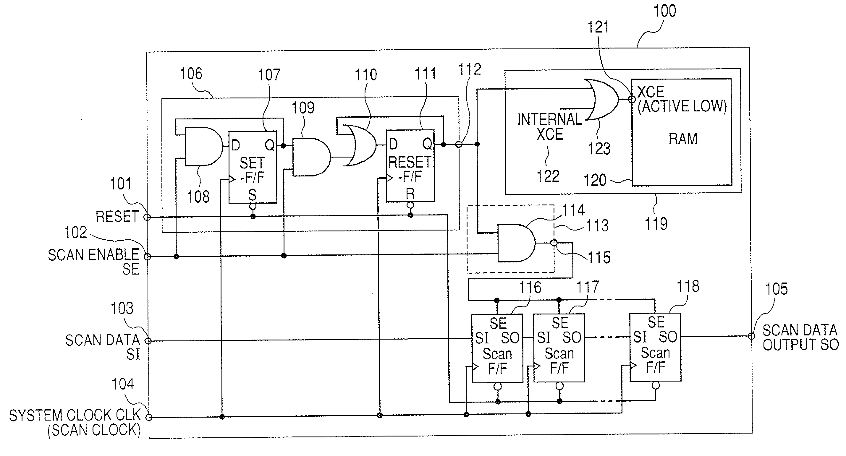
[0068]FIG. 1 is a view illustrating a circuit configuration of a first exemplary embodiment in the present invention. As in the case of FIG. 7 of a conventional example, FIG. 1 also does not illustrate a circuit system corresponding to an internal circuit 601 illustrated in FIG. 6, namely, a logic circuit system to be used in a normal operation; and illustrates only a part which directly relates to the present invention.

[0069]Accordingly, scan-FFs 116 and 117 each shall have a normal operation data input section (D) connected to a normal operation data input terminal (not shown). In addition, reference character SO of the n-th last scan-FFN outputs a data of a normal operation as well.

[0070]A semiconductor integrated circuit 100 has a scan data input terminal 103 and a scan data output terminal 105 arranged therein. N sets of scan-FFs from a scan-FF116 to a scan-N (for instance, when n=3, N=FF118) from a scan chain between the scan data input terminal 103 and the scan data output te...

second embodiment

[0141]FIG. 4 is a view illustrating a circuit configuration of a second exemplary embodiment in the present invention.

[0142]FIG. 4 illustrates a configuration which has scan-FFs 402 to 409 arranged for inputting a signal into an internal circuit 401 of a semiconductor integrated circuit 400 and receiving an output from the internal circuit 401.

[0143]In the present exemplary embodiment, a scan enable signal is input into a scan-FF405 as a normal data input IN4, and is also input into a decision circuit 410 which has been described in Exemplary embodiment 1. This point is different from that in Exemplary embodiment 1.

[0144]The present exemplary embodiment has thus configuration of inputting the output of the decision circuit into a mask circuit 411 also shown in the above described Exemplary embodiment 1, and connecting the output of the mask circuit 411 to a scan enable input of scan-FFs 402 to 409.

[0145]The normal operation and the scan test can be carried out by using the decision ...


PUM


Abstract

A semiconductor integrated circuit comprises a test mode decision circuit which decides a normal operation mode or a test mode when having input a clock from a reset state and started an operation by using a scan enable signal that is used for a scan test, and retains a decision result till the decision result is reset; a scan enable mask circuit which disables the transmission of a scan enable signal to an internal scan circuit according to a decision result signal; and an access control unit which disables the access to the internal memory unit according to the decision result signal output from the test mode decision circuit. Furthermore, the semiconductor integrated circuit has a configuration of using the scan enable signal and the normal operation input signal in common.

Description

BACKGROUND OF THE INVENTION[0001]1. Field of the Invention[0002]The present invention relates to a semiconductor integrated circuit such as an LSI, in particular, relates to a semiconductor integrated circuit having a scan circuit arranged therein.[0003]2. Description of the Related Art[0004]A semiconductor integrated circuit such as an LSI conventionally has a scan circuit therein which is arranged for the purpose of determining whether the semiconductor integrated circuit has a defect formed in a manufacturing process or not. For instance, Japanese Patent Application Laid-Open No. S63-134970 and Japanese Patent Application Laid-Open No. H04-072583 describe a testing technique with the use of the scan circuit.[0005]The scan circuit uses a scan flip-flop (hereafter referred to as an FF) as shown in FIG. 5, for instance.[0006]FIG. 5 illustrates a configuration for forming a scan-FF by using a flip-flop (hereafter referred to as an FF) provided with a reset terminal.[0007]A multiplex ...

Claims


Application Information

Patent Timeline
IPC IPC(8): G01R31/28
CPCG01R31/318555G01R31/31719G11C29/00
Inventor YAMAZAKI, TATSUHIKO
Owner CANON KK
Why Eureka
Try Eureka