Current Detection Circuit and Switching Power Supply Using the Same

a current detection circuit and switching power supply technology, applied in the direction of power conversion systems, dc-dc conversion, instruments, etc., can solve the problems of reduced efficiency, loss of conductance, and inability to detect the reverse current flowing in the conventional current detection circuit configured as described above, and achieve the effect of improving the transient response characteristics

Active Publication Date: 2008-01-24
PANASONIC SEMICON SOLUTIONS CO LTD
View PDF6 Cites 18 Cited by
  • Summary
  • Abstract
  • Description
  • Claims
  • Application Information

AI Technical Summary

Benefits of technology

[0007] The present invention is intended to provide a current detection circuit capable of detecting the reverse current flowing in a switching device and to provide a switching power supply, the transient response characteristics of which are improved by using this current detection circuit.
[0011] a compensation circuit for adjusting the output current of the auxiliary switching device so that the potential obtained by adding the offset voltage to the output potential of the switching device becomes equal to the output potential of the auxiliary switching device. The current detection circuit in accordance with the present invention configured as described above can accurately detect the reverse current flowing in the switching device.
[0020] a compensation circuit for adjusting the output current of the auxiliary switching device so that the potential obtained by adding the offset voltage to the output potential of the switching device becomes equal to the output potential of the auxiliary switching device. The switching power supply in accordance with the present invention configured as described above has excellent transient response characteristics by using the current detection circuit capable of detecting the reverse current flowing in the switching device.
[0025] The current detection circuit in accordance with the present invention can surely detect the reverse current flowing in the switching device by using a simple configuration.
[0027] Furthermore, in the switching power supply using the current detection circuit in accordance with the present invention and conforming to the current mode control system, the change width of the setting value of the operation current is limited to the necessary minimum during the ordinary operation, and the limitation in the change width of the setting value of the operation current is relaxed during a transient period, for example, when the output conditions change abruptly. Hence, the switching power supply produces excellent effects of quickening responsiveness and smoothing return to the ordinary operation.
[0028] Still further, in the switching power supply using the current detection circuit in accordance with the present invention and conforming to the current mode control system, the offset level of the current detection circuit is made variable. During a transient period, for example, when the output conditions change abruptly, the offset level is set at a large value, whereby the detection level is shifted. Hence, the switching power supply has excellent effects of quickening responsiveness and smoothing return to the ordinary operation.

Problems solved by technology

In the case that a current detection device, such as a resistor, is used in a current detection circuit, a conduction loss occurs and its efficiency is reduced.
In other words, the conventional current detection circuit configured as described above cannot detect the reverse current flowing in the switching device of the switching power supply.

Method used


Image

  • Current Detection Circuit and Switching Power Supply Using the Same
  • Current Detection Circuit and Switching Power Supply Using the Same
  • Current Detection Circuit and Switching Power Supply Using the Same

Examples


first embodiment

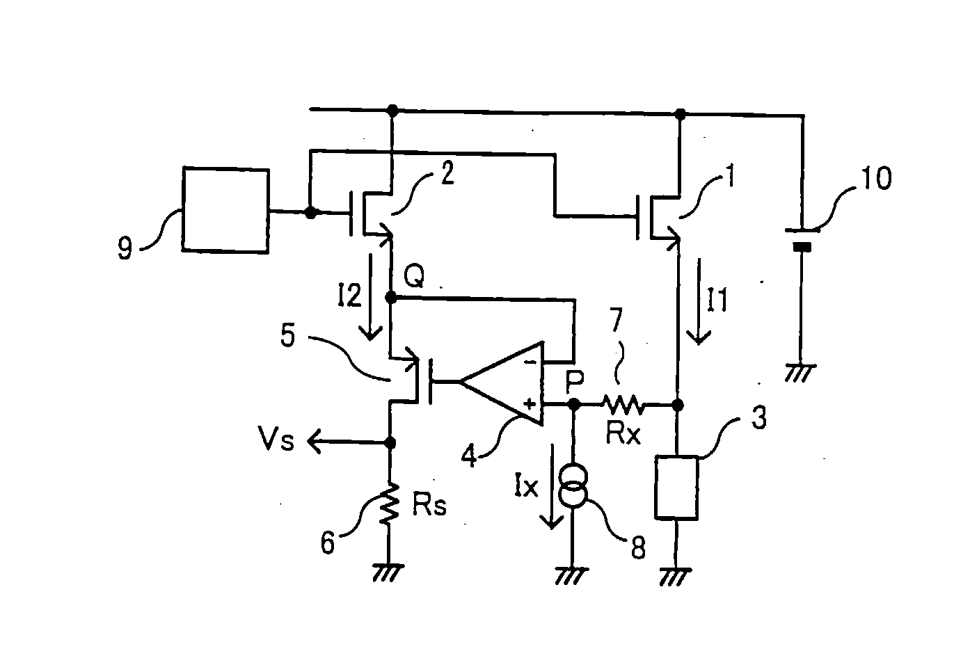
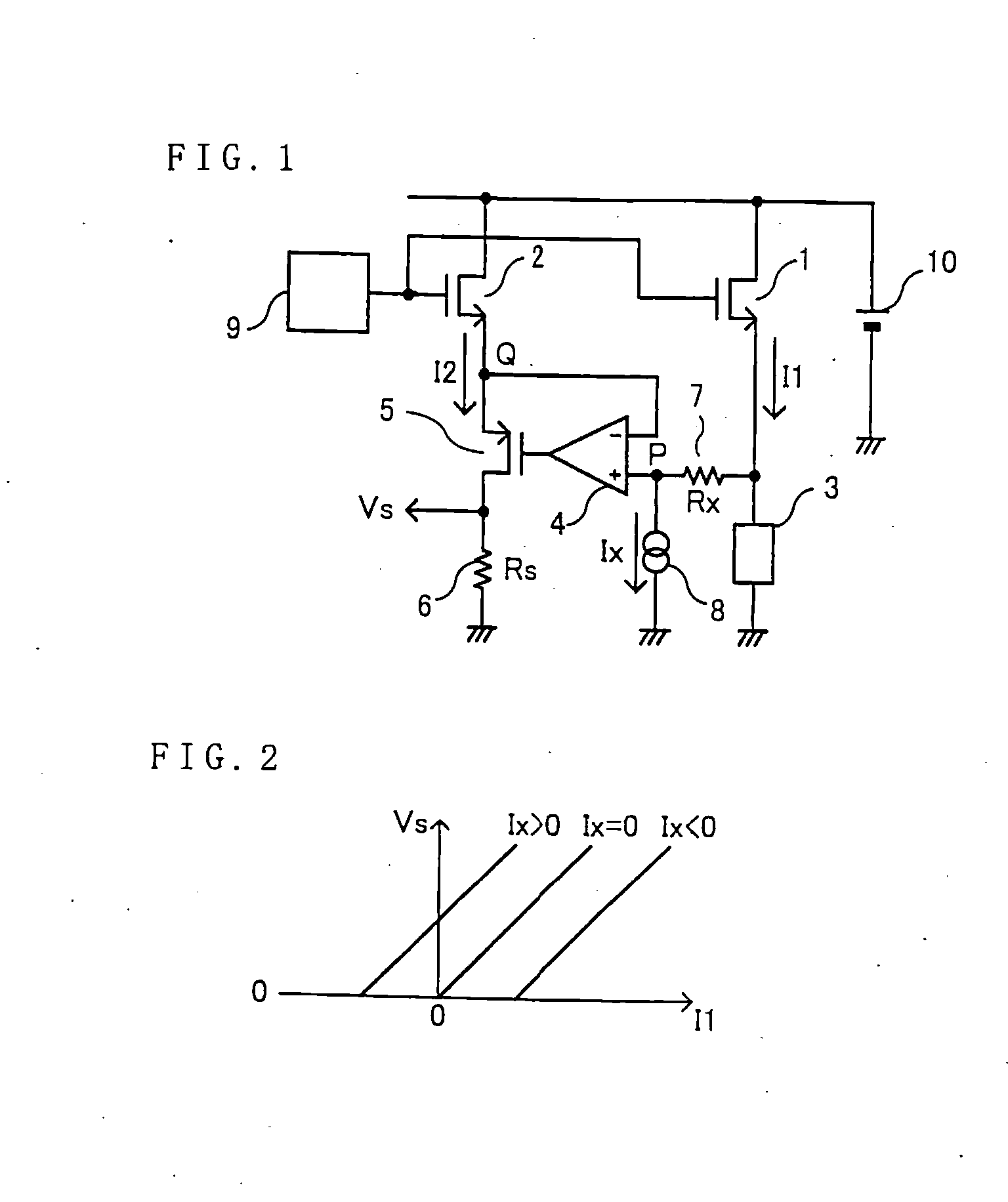
[0043]FIG. 1 is a circuit diagram showing the configuration of a current detection circuit in accordance with a first embodiment of the present invention. In the current detection circuit in accordance with the first embodiment, an output transistor 1 is a switching device and formed of an N-channel MIS FET (metal insulator semiconductor field effect transistor). An auxiliary transistor 2, connected in parallel with the output transistor 1, is formed of an N-channel MIS FET. In addition, a compensation transistor 5 is formed of a P-channel MIS FET. In FIG. 1, numeral 3 designates a load, numeral 4 designates a differential amplifier, numeral 6 designates a current detection resistor, numeral 7 designates an offset resistor device, numeral 8 designates a current source circuit, numeral 9 designates a drive circuit, and numeral 10 designates a DC power supply.

[0044] The drain of the output transistor 1 is connected to the DC power supply 10, the gate thereof is connected to the drive...

second embodiment

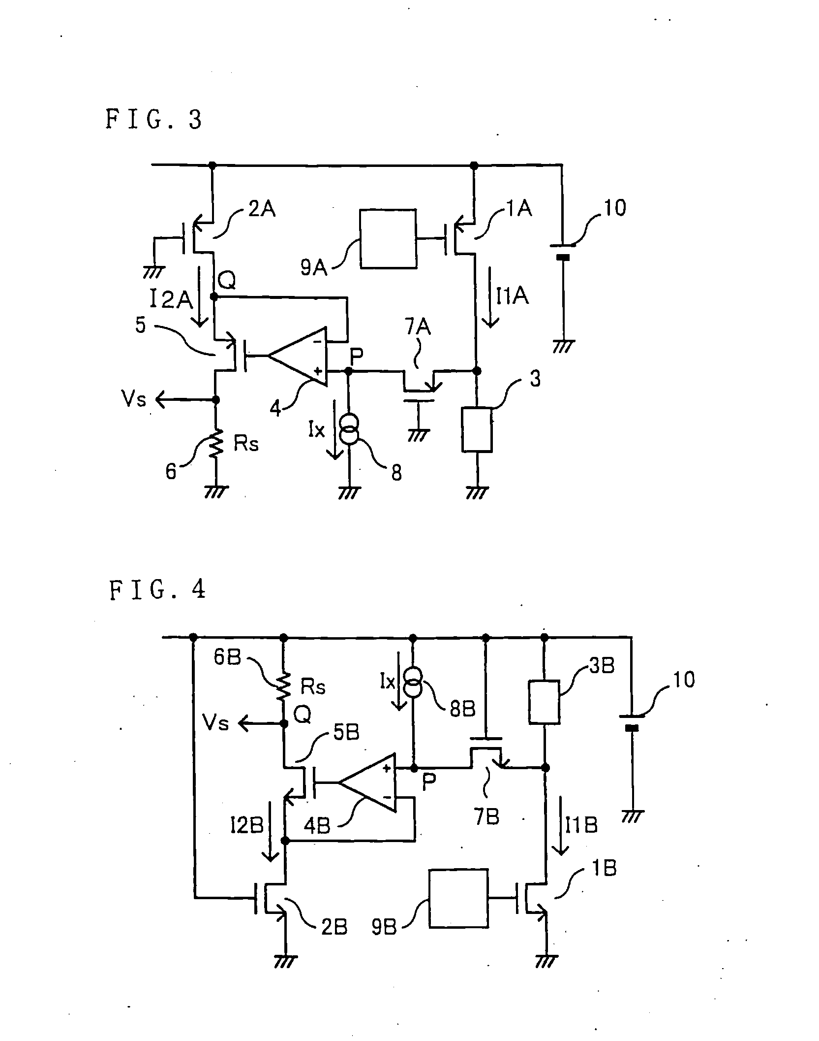
[0056] A current detection circuit in accordance with a second embodiment of the present invention will be described below using the accompanying drawing, FIG. 3. FIG. 3 is a circuit diagram showing the configuration of the current detection circuit in accordance with the second embodiment.

[0057] In FIG. 3, numeral 1A designates an output transistor serving as a switching device and formed of a P-channel MIS FET. Numeral 2A designates an auxiliary transistor formed of a P-channel MIS FET. Numeral 3 designates a load, numeral 4 designates a differential amplifier, numeral 5 designates a compensation transistor formed of a P-channel MIS FET, numeral 6 designates a current detection resistor, numeral 7A designates an offset resistor device formed of a P-channel MIS FET, numeral 8 designates a current source circuit, numeral 9 designates a drive circuit, and numeral 10 designates a DC power supply. The configuration of the current detection circuit in accordance with the second embodim...

third embodiment

[0066] A current detection circuit in accordance with a third embodiment of the present invention will be described below using the accompanying drawing, FIG. 4. FIG. 4 is a circuit diagram showing the configuration of the current detection circuit in accordance with the third embodiment of the present invention.

[0067] As shown in FIG. 4, in the current detection circuit in accordance with the third embodiment, a load 3B is connected to the power supply potential side. An output transistor 1B serving as a switching device is formed of an N-channel MIS FET, the source of which is grounded. In FIG. 4, an auxiliary transistor 2B, a compensation transistor 5B and an offset resistor device 7B are all formed of an N-channel MIS FET. The gates of the auxiliary transistor 2B and the offset resistor device 7B have the power supply potential Vi, and the source of the auxiliary transistor 2B is grounded. A current source circuit 8B is configured to pass a current to the offset resistor device...


PUM


Abstract

A current detection circuit of the present invention has a switching device 1; an auxiliary switching device 2; an offset voltage source comprising an offset resistor device 7 and a current source circuit 8; a compensation circuit, comprising a differential amplifier 4 and a compensation transistor 5, for adjusting the output current of the auxiliary switching device 2 so that the potential obtained by subtracting the voltage drop across the offset resistor device 7 from the output potential of the switching device 1 is equal to the output potential of the auxiliary switching device 2, being configured that the detection level of the current flowing in the switching device 1 is shifted by an offset amount.

Description

BACKGROUND OF THE INVENTION [0001] The present invention relates to a current detection circuit for detecting the current flowing in a switching device, such as a MIS FET (metal insulator semiconductor field effect transistor), and a switching power supply using the same. [0002] In recent years, switching power supplies have been used in various electronic apparatuses because of their high efficiency and high power conversion characteristics. In particular, in the case that quick transient response characteristics are requested, the current mode control system, which is not affected by the resonance frequency of an inductor and an output capacitor constituting such a switching power supply, is used. The current mode control system detects the current flowing in the inductor and controls the current to carry out output control, and requires a current detection circuit. In the case that a current detection device, such as a resistor, is used in a current detection circuit, a conductio...

Claims


Application Information

Patent Timeline
Patent Type & Authority Applications(United States)
IPC IPC(8): G05F1/10
CPCH02M2001/0009H02M3/156H02M1/0009
Inventor RYU, TAKASHIISHII, TAKUYAMOTOMORI, MIKIOTANABE, HIROHISASHIGEMI, TOMOYA
Owner PANASONIC SEMICON SOLUTIONS CO LTD
Why Eureka
Try Eureka