Liquid crystal display device

a technology of liquid crystal display and display device, which is applied in the direction of optics, non-linear optics, instruments, etc., can solve the problems of insufficient adhesiveness of sealing agent and tft substrate, difficult to restrict and difficult to control the position of the outer periphery of the applied region formed, so as to prevent spreading

Active Publication Date: 2008-01-24
PANASONIC LIQUID CRYSTAL DISPLAY CO LTD +1
View PDF9 Cites 48 Cited by
  • Summary
  • Abstract
  • Description
  • Claims
  • Application Information

AI Technical Summary

Benefits of technology

[0013]In forming the orientation film using the inkjet printing method, to prevent the printed orientation film material ink from spreading by wetting to the sealing region, it may be possible to provide a method which preliminarily decreases a region on which the orientation film material is printed by taking a spreading-by-wetting quantity of the printed orientation material ink into consideration. However, this method results in narrowing an effective display region and, is liable to generate irregularities in a film thickness of the orientation film printed in the inside of the display region.
[0014]Besides such a method, it may be also possible to provide a method which suppresses spreading by wetting of the orientation film material ink to be printed by increasing the viscosity of the orientation material ink. However, this method is liable to easily form a region where the orientation film material ink is not applied due to an injection failure (clogging of a nozzle) at the time of printing.
[0015]It is an object of the present invention to provide a liquid crystal display device having the structure which, for example, in forming an orientation film in a manufacturing process of a liquid crystal display panel, can suppress undesired spreading by wetting of an orientation film material in an outer peripheral portion of a display region and, at the same time, can maintain the uniformity of a film thickness of the orientation film within the display region.
[0018]The surface of the region in the extending direction of the signal lines (particularly, the scanning signal lines) formed on the substrate, that is, in the direction for pulling out the signal line to a drive circuit from the display region has small irregularities. By forming the recessed groove in such a portion, it is possible to prevent spreading by wetting of the orientation film material ink.

Problems solved by technology

However, in forming the orientation film using the ink jet printing method, it has been pointed out that it is difficult to restrict a position of a periphery of an ink applied region.
That is, the viscosity of orientation-film-material ink used in the ink jet printing method is low compared to the viscosity of a material used in the aniline printing method and hence, when the material of the resin film which forms the orientation film by the ink jet method is applied to the substrate, it is difficult to control the position of the outer periphery of the applied region formed along with spreading by wetting of the orientation material ink which is discharged to the substrate from a nozzle of an ink jet device.
The orientation film reaches the sealing region, the adhesiveness of the sealing agent and the TFT substrate becomes insufficient attributed to the presence of the orientation film material below the sealing agent and the substrate.
This insufficient adhesiveness gives rise to the defective sealing, the positional displacement with the counter substrate or leaking of a liquid crystal material.
However, this method results in narrowing an effective display region and, is liable to generate irregularities in a film thickness of the orientation film printed in the inside of the display region.
However, this method is liable to easily form a region where the orientation film material ink is not applied due to an injection failure (clogging of a nozzle) at the time of printing.

Method used


Image

  • Liquid crystal display device
  • Liquid crystal display device
  • Liquid crystal display device

Examples


embodiment 1

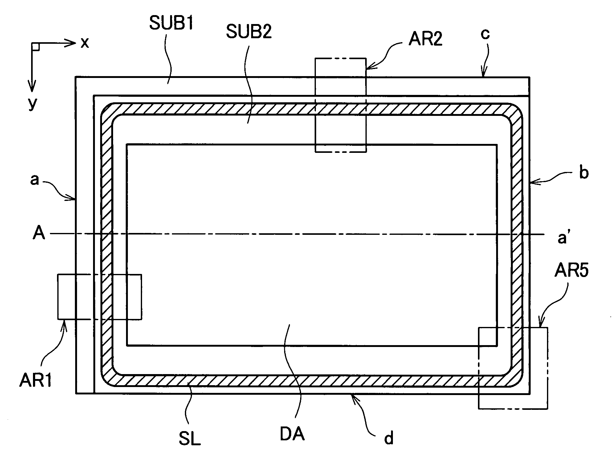
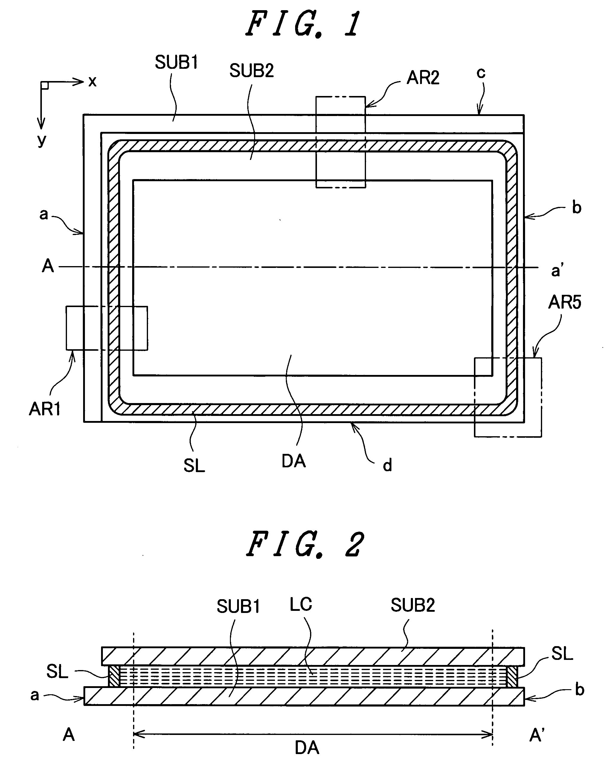
[0049]FIG. 1 is a schematic plan view showing the schematic constitution of a liquid crystal display panel of an embodiment 1 according to the present invention. Further, FIG. 2 is a cross-sectional view taken along a line A-A′ in FIG. 1. The liquid crystal display device of the embodiment 1 is constituted of the liquid crystal display panel which includes a first substrate SUB1 which forms one of substrates which are adhered to each other, a second substrate SUB2 which forms another substrate, a sealing region SL which is arranged annularly along a periphery of a gap defined between opposing surfaces of the first substrate SUB1 and the second substrate SUB2, and a liquid crystal layer which is sealed in a space surrounded by the first substrate, and the second substrate and the sealing region, wherein a display region DA is formed inside the sealing region. The display region DA for displaying a video or an image is formed in a region where the first substrates SUB1, the second sub...

embodiment 2

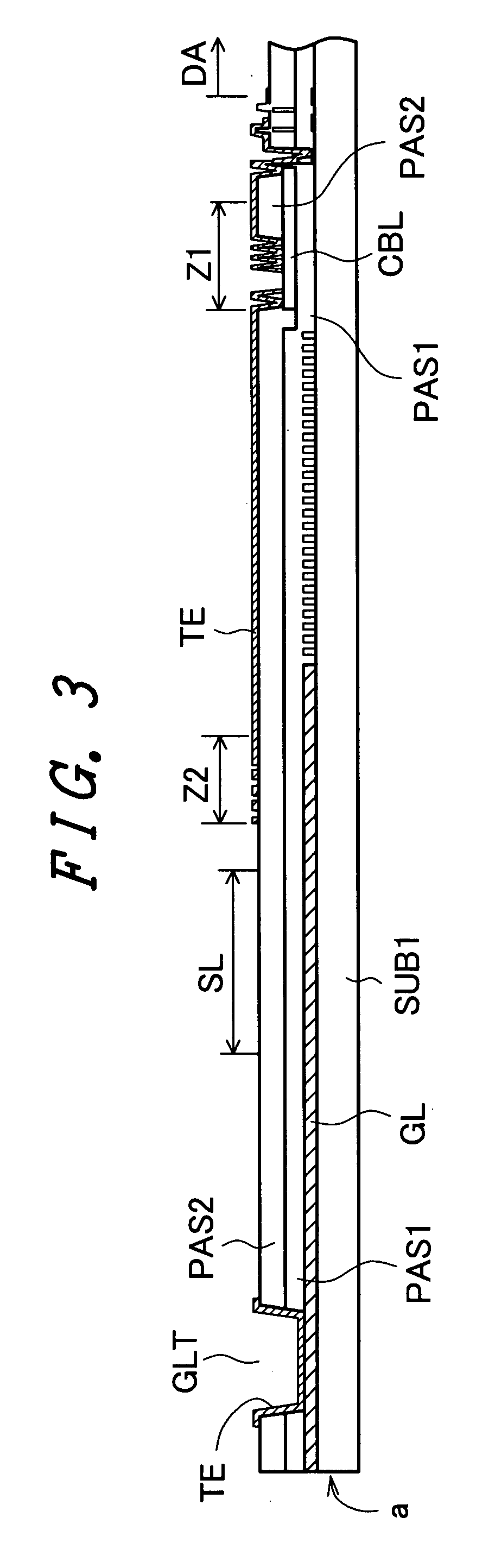
[0067]FIG. 10 is a plan view of an essential part of a drain side of a TFT substrate indicated by symbol AR2 in FIG. 1 which schematically shows the schematic constitution of a liquid crystal display panel of an embodiment 2 according to the present invention. Further, FIG. 11 is a schematic plan view showing the schematic constitution of a region AR3 shown in FIG. 10 in an enlarged manner. FIG. 12 is a schematic cross-sectional view taken along a line D-D′ in FIG. 11. FIG. 13 is a schematic plan view showing the schematic constitution of a region AR4 shown in FIG. 10 in an enlarged manner. FIG. 14 is a schematic cross-sectional view taken along a line E-E′ in FIG. 13.

[0068]In the liquid crystal display panel of this embodiment, to observe an outer peripheral portion of the display region DA of the TFT substrate SUB1 close to the drain side c in an enlarged manner, as shown in FIG. 10, outside the display region DA, a common bus line CBL is formed along the outer periphery of the di...


PUM

PropertyMeasurementUnit
conductiveaaaaaaaaaa
sizeaaaaaaaaaa
viscosityaaaaaaaaaa

Abstract

The present invention suppresses the spreading by wetting of an orientation film material in a liquid form toward a sealing agent applied region positioned on an outer periphery of a display region in forming an orientation film thus ensuring the uniformity of a film thickness in the display region. A pair of substrates includes orientation films on surfaces thereof which face opposing substrates. Out of the pair of substrates, the substrate on which the signal lines are formed, on a side thereof which is disposed between a region on which the sealing material is arranged and the display region and along which the signal lines extend to the outside of the sealing material from the display region, includes a first conductive layer, a second conductive layer and an insulation layer which is interposed between the first and second conductive layers between the orientation film and the substrate, the insulation layer extends in the direction at least along an outer periphery of the display region, and includes groove portion having a recessed groove which opens on the orientation film side, the first conductive layer is formed along a shape of the recessed groove, and the signal lines are formed in a state that the signal lines go around the recessed groove.

Description

[0001]The present application claims priority from Japanese application JP2006-195104 filed on Jul. 18, 2006, the content of which is hereby incorporated by reference into this application.BACKGROUND OF THE INVENTION[0002]1. Field of the Invention[0003]The present invention relates to a liquid crystal display device, and more particularly to a technique suitable for a control of an outer periphery of an orientation film material in applying an orientation film to an inner surface of a substrate of a liquid crystal display panel which constitutes a liquid crystal display device.[0004]2. Description of the Related Art[0005]As a television device or a display device of an information terminal, a liquid crystal display device which uses a liquid crystal display panel sealing a liquid crystal material between a pair of substrates consisting of a first substrate and a second substrate has been widely spreading. Usually, the liquid crystal display panel which constitutes this type of liqui...

Claims


Application Information

Patent Timeline
Patent Type & Authority Applications(United States)
IPC IPC(8): G02F1/1339G02F1/1343
CPCG02F1/133711G02F2001/133388G02F1/1339G02F1/133388G02F1/1345G02F1/13
Inventor IWATO, HIROAKIICHIHARA, KATSUMIHIRATA, MASAFUMIKURAHASHI, NAGATOSHI
Owner PANASONIC LIQUID CRYSTAL DISPLAY CO LTD
Why Eureka
Try Eureka