Access time adjusting circuit and method for non-volatile memory

Active Publication Date: 2008-01-24
SOLID STATE SYST
View PDF5 Cites 11 Cited by
  • Summary
  • Abstract
  • Description
  • Claims
  • Application Information

AI Technical Summary

Benefits of technology

[0007]The invention provides access time adjusting circuit and method for improving the performance for the non-volatile memory device by optimizing the operation clock with respect to one memory being chosen by an user.
[0008]The invention provides access time adjusting circuit and method for improving the performance for the non-volatile memory device, in which an optimized operation clock can be obtained by trigger or by automatic adjustment. The variation due to environment factor can also be reduced.
[0028]The present invention propose an circuit or a method to adaptively adjust the operation clock for improving the performance of the memory in different type.

Problems solved by technology

To speed up the Flash Access, performance is an important issue in many Flash Application such as DSC (Digital Still Camera), UFD (USB Flash Disk), Mobile Phone, et al.
Although users do their best, there is a limitation in the Flash Access Timing Specification, on which users must follow to guarantee the Flash Data Access Correctness.
However in real usage, there are a lot of margins in the access time.

Method used


Image

  • Access time adjusting circuit and method for non-volatile memory
  • Access time adjusting circuit and method for non-volatile memory
  • Access time adjusting circuit and method for non-volatile memory

Examples


Embodiment Construction

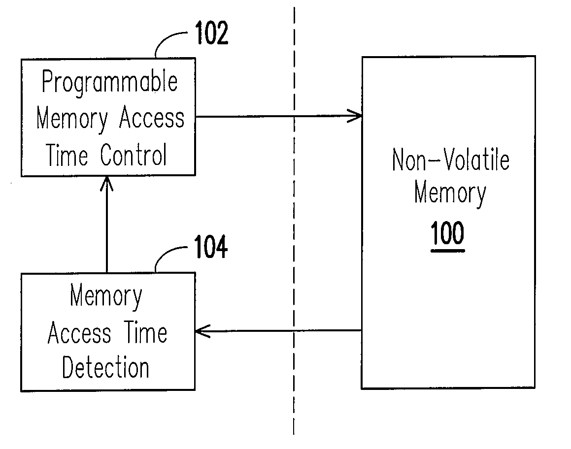
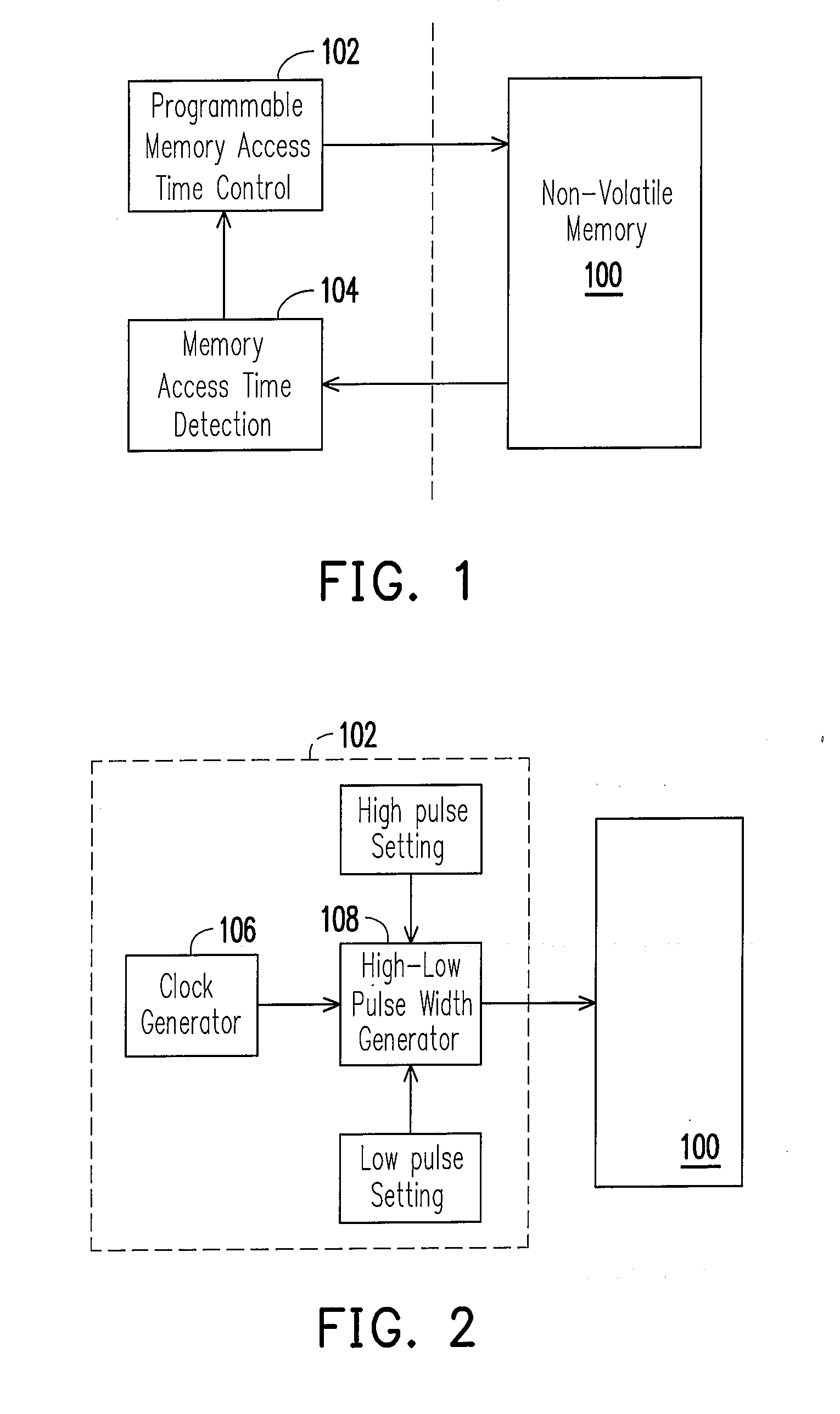
[0035]In the invention, a novel access time adjusting circuit and method is proposed. The invention can be, for example, specifically used in “NAND Type Flash Access Time Control”. However, the present invention can generally adjust the access time for a non-volatile memory to improve the performance from the default setting. Several embodiments are provided for describing the features of the invention. However, the invention is not limited to the embodiments.

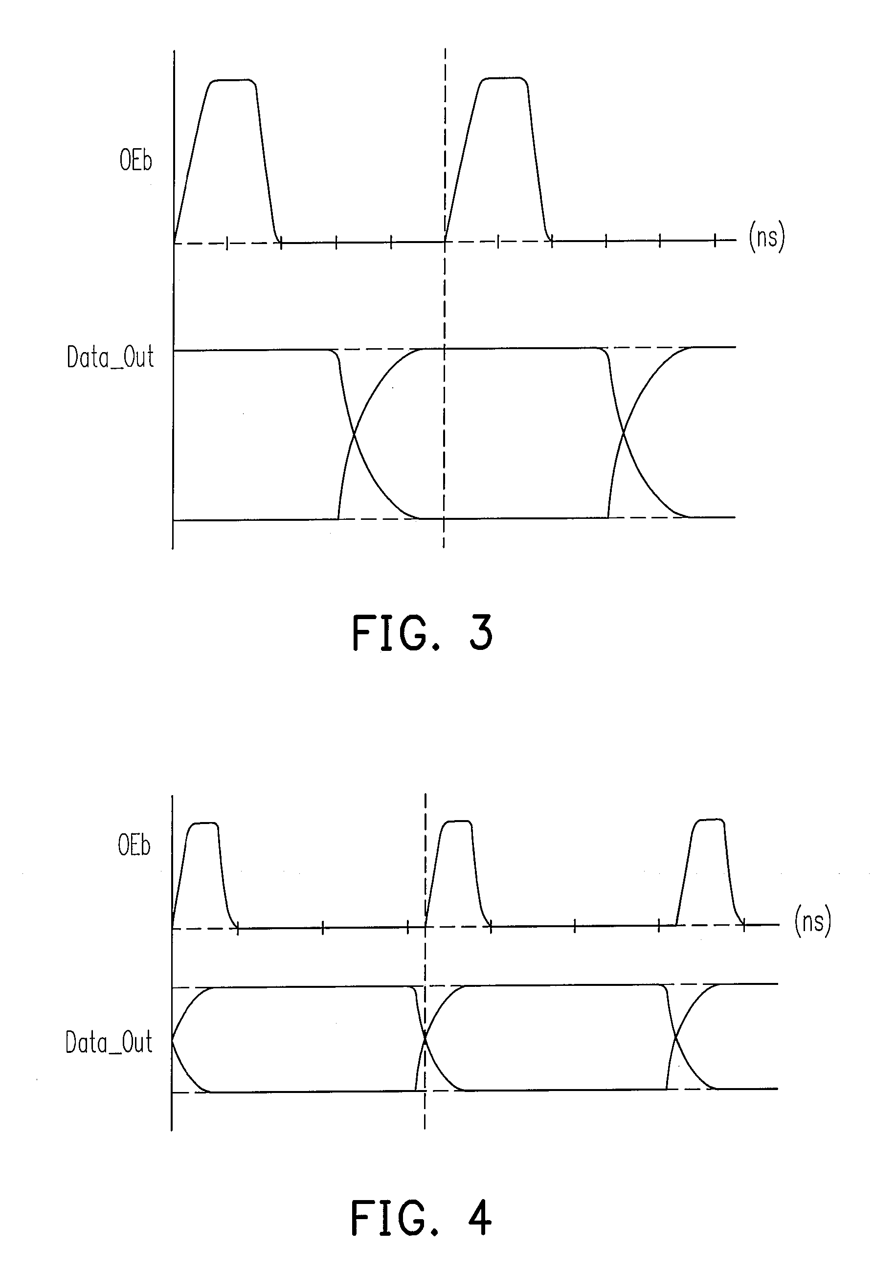
[0036]FIG. 1 is a block diagram, schematically illustrating the access time adjusting circuit, according to an embodiment of the invention. In FIG. 1, a non-volatile memory 100, such as the flash memory, basically has the specific operation clock at a relatively lower speed, so as to ensure the memory 100 to be accessed without causing error. However, at this relatively lower speed, the performance of the memory 100 is not at the good condition. Usually, the memory 100 can be operated in faster speed. The invention can optimize...


PUM


Abstract

An access time adjusting circuit is used in a non-volatile memory to obtain an optimized access time in operation. The circuit includes an access time detecting unit, used to detect a performance status of the non-volatile memory under an operation clock and output the performance status. An access time controlling unit is used to generate at least one adjusting operation clock. Each the adjusting operation clock serves as the operation clock for the non-volatile memory. In addition, the non-volatile memory, the access time controlling unit, and the access time detecting unit are connected to form a detection and adjustment loop, so that an optimized operation clock is determined after checking the at least one adjusting operation clock.

Description

BACKGROUND OF THE INVENTION[0001]1. Field of Invention[0002]The present invention relates to technology for accessing a non-volatile memory. More particularly, the present invention relates to an accessing time adjustment for accessing a non-volatile memory.[0003]2. Description of Related Art[0004]Memory device in digital apparatus or digital is a necessary part. There are many kinds of non-volatile memory, such as NAND Type Flash devices, in the market for choice to the user. Taking the flash memory as the example, for different flash memory provider, the access time specification of the flash memory may be different. Even for the same Flash provider, although the Flash Access Time specification is the same, for the different Semiconductor Process, the “Real Acceptable Flash Access Time” has a lot of margin, compared to the timing rated in the specification. Even for the same Flash device, due to the operating voltage and thermal temperature variation, the Flash Access speed may be...

Claims


Application Information

Patent Timeline
IPC IPC(8): G11C8/00
CPCG11C2207/2254G11C16/32
Inventor LIN, GENE
Owner SOLID STATE SYST
Why Eureka
Try Eureka