Process for Producing Printed Articles
- Summary
- Abstract
- Description
- Claims
- Application Information
AI Technical Summary
Benefits of technology
Problems solved by technology
Method used
Image

Examples
example 1
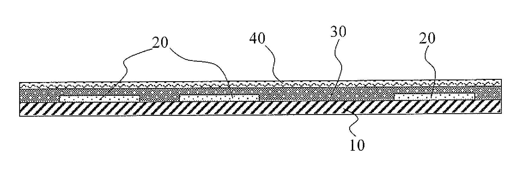
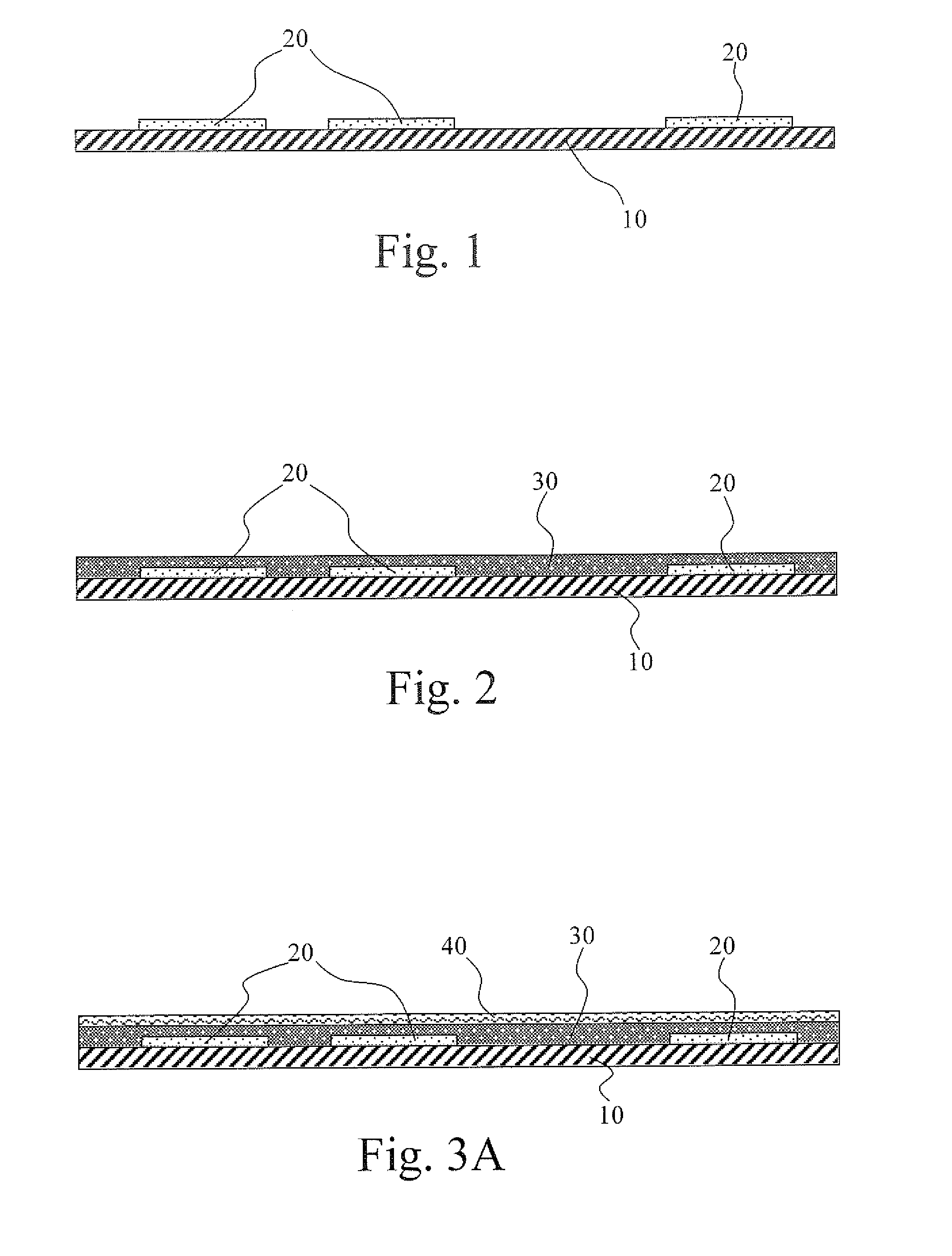
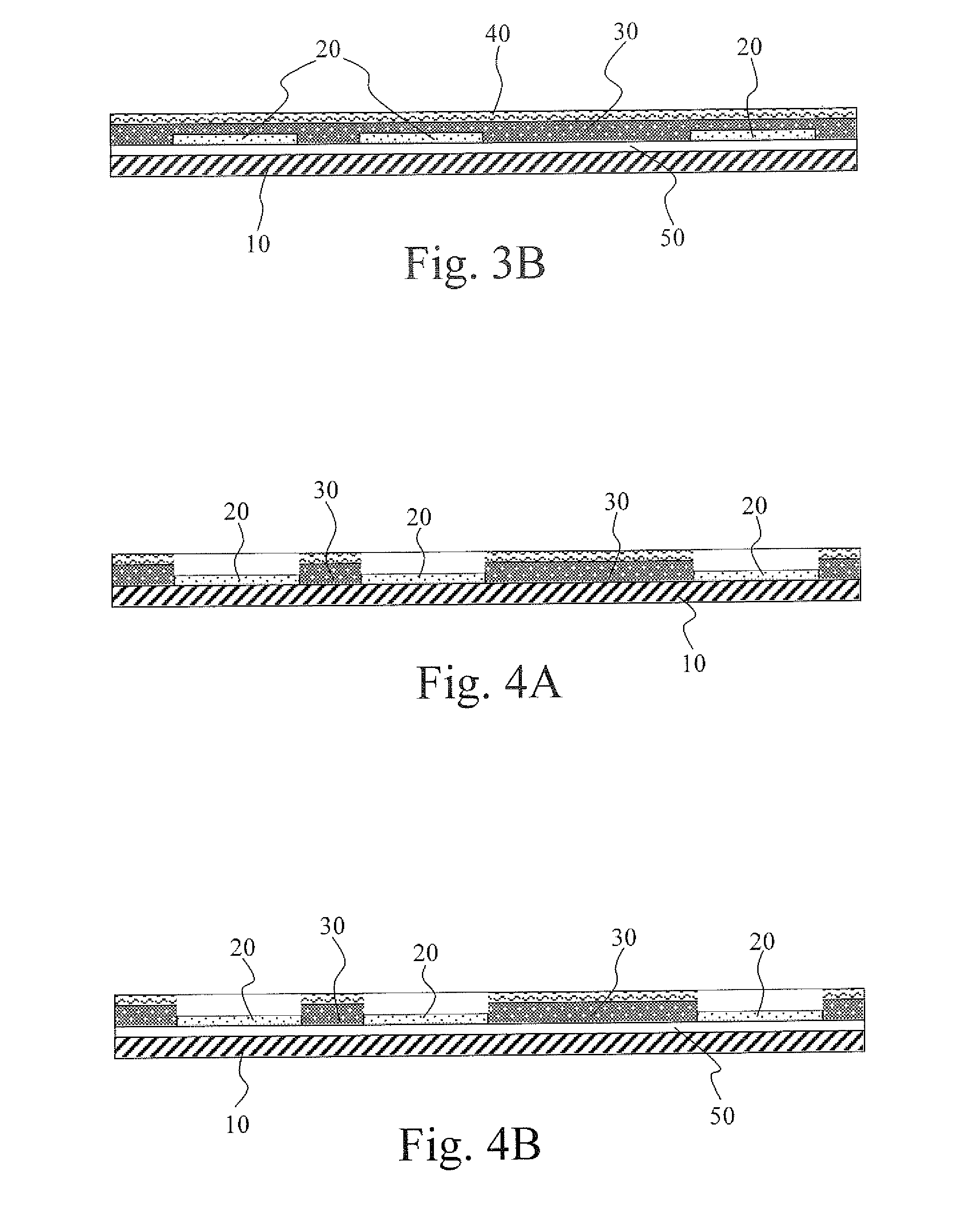
[0031] Matt coated paper weighing 90 g., produced by the Burgo paper mill, was used as printing support 10.
[0032] The characters 20 were printed using the “dry offset” method with a transparent ink called Deltacote 12800 produced by the Colorgraf company, with the addition of the article “Release 202067” in a proportion of 30% to 70% by volume.
[0033] The characters 20 were then overprinted with a second, colored ink 30 of the UV-dried type called XPRESS and produced by the Colorgraf company. The ink layer 30 was applied using the lithographic offset method.
[0034] Overprinting with the transparent varnish 40 using appropriate graphics was done with a closed-chamber flexographic printing system. The security texture was chosen so as to reproduce the hidden characters repeated and overlaid with a screen ruling of 30%, 60% and 80%.
[0035] From the observation of the articles thus obtained it was not possible to distinguish the hidden characters through the paint. Removal of the upper...
example 3
[0037] Ordinary paper weighing 80 g. was used after treating the surface to be printed first with a “primer” called Release Dry Offset produced by Colorgraf.
The process described in Example 1 was then used to obtain printed articles with characteristics similar to those of Examples 1 and 2.
PUM
| Property | Measurement | Unit |
|---|---|---|
| Time | aaaaa | aaaaa |
| Transparency | aaaaa | aaaaa |
| Plasticity | aaaaa | aaaaa |
Abstract
Description
Claims
Application Information
PatSnap Eureka turns technology decisions into work you can execute. Powered by our Innovation Knowledge Graph, it runs expert workflows across engineering, life sciences, materials and intellectual property. Get your review-ready output in minutes.


