
Integrated circuit

Inactive Publication Date: 2008-02-21
FUJITSU LTD
View PDF5 Cites 2 Cited by
  • Summary
  • Abstract
  • Description
  • Claims
  • Application Information

AI Technical Summary

Benefits of technology

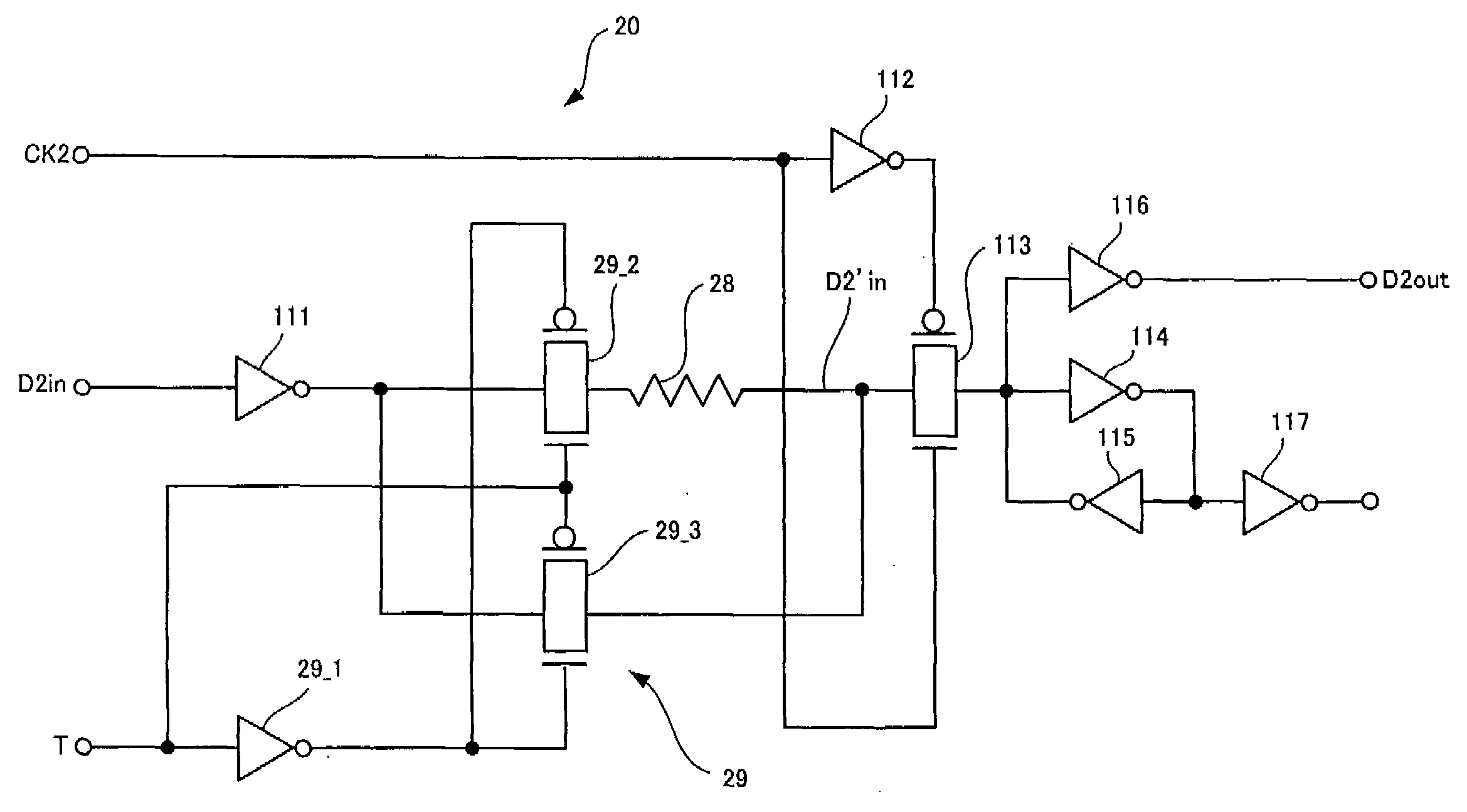
[0027]According to the first integrated circuit of the present invention, the second latch comprises: a delay element that delays an input signal transmitted from the first latch; and a path switching circuit that changes over a signal input path in such a way that at time of a usual operation, the input signal is taken through bypassing the delay element and at time of a test operation, the input signal is taken via the delay element. This feature makes it possible to discriminate between the defective holding and the stack breakdown by an LSI tester.
[0031]Those features make it possible to implement the delay element simply.
[0035]According to the second integrated circuit of the present invention, the second latch comprises: the input buffer that buffers an input signal transmitted from the first latch; and the back bias applying circuit that applies a back bias to the input buffer at time of a test operation. This feature makes it possible to delay the signal when the back bias is applied to the output buffer, so that the same effect as the delay element by the first integrated circuit is caused. Thus, according to the second integrated circuit of the present invention, it is possible to discriminate between the defective holding and the stack breakdown by an LSI tester.
[0039]According to the third integrated circuit of the present invention, the first latch comprises: the output buffer that buffers a signal outputted from the first latch; and the back bias applying circuit that applies a back bias to the output buffer at time of a test operation. This feature makes it possible to delay the signal from the output buffer when the back bias is applied to the output buffer, so that the same effect as the delay element by the first integrated circuit is caused. Thus, according to the third integrated circuit of the present invention, it is possible to discriminate between the defective holding and the stack breakdown by an LSI tester.

Problems solved by technology

Even if the technology disclosed in Japanese Patent Publication TokuKai 2005-293622 mentioned above is adopted so that the margin of the holding time is evaluated to reflect the evaluation result, the large margin may involve the decrease at operation speed, and thus it is difficult to omit the possibility that defective holding is generated owing to the manufacturing process etc.
According to the conventional integrated circuit, it is difficult that an LSI tester is used to discriminate between the defective holding and the stack breakdown.
However, according to the conventional integrated circuit, it is difficult to discriminate between the defective holding and the stack breakdown.
Thus, it is difficult to feed back information as to defective holding even to the design phase of the integrated circuit.

Method used


Image

  • Integrated circuit
  • Integrated circuit
  • Integrated circuit

Examples


first embodiment

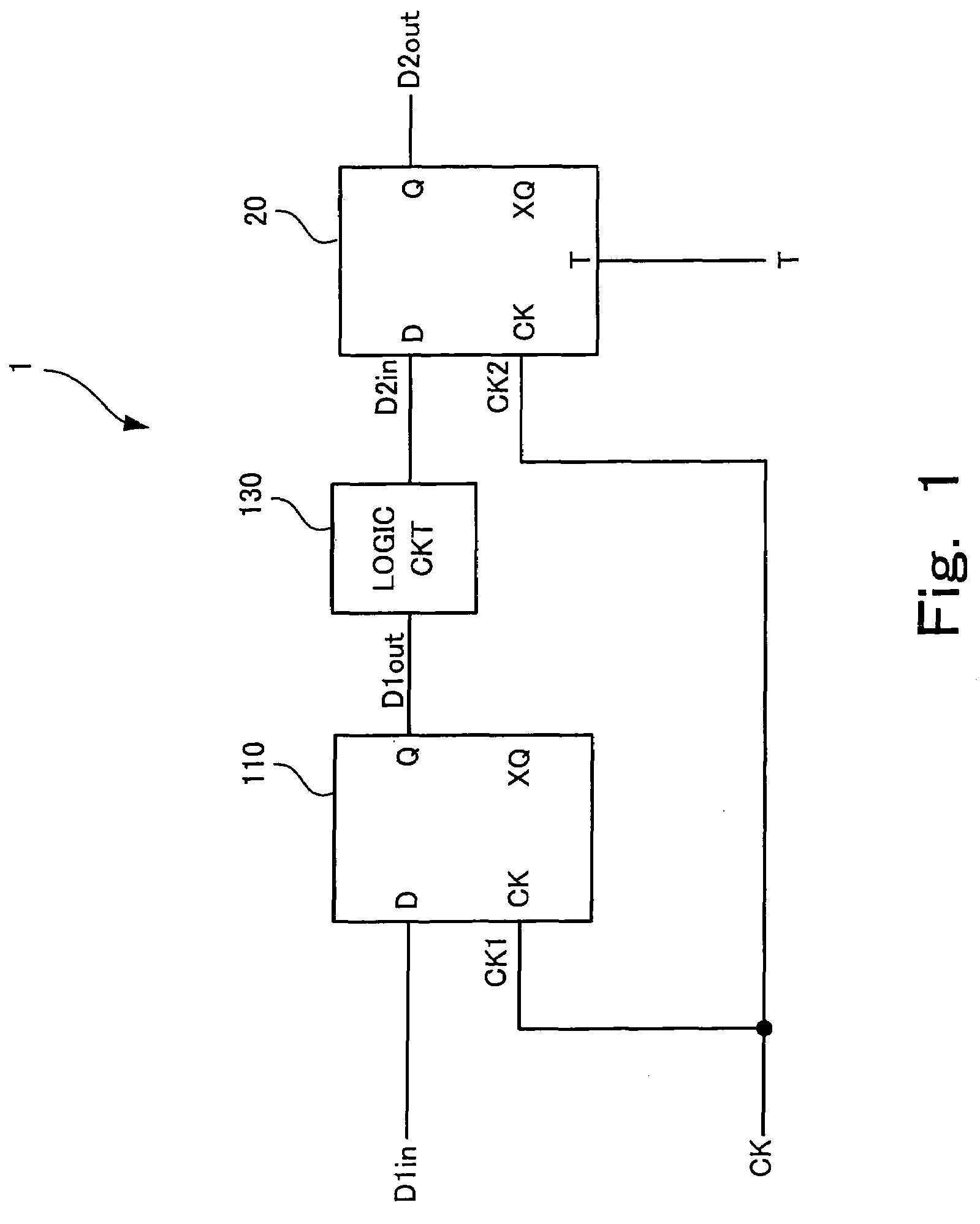
[0052]FIG. 1 is a block diagram showing a structure of a first integrated circuit of the present invention.

[0053]An integrated circuit 1 shown in FIG. 1 comprises the first latch 110 of a data transmitting source, which is the same as one shown in FIG. 9, a second latch 20 of a data receiving destination, which is the feature of the present embodiment, and a logic circuit 130 disposed between the first latch 110 and the second latch 20. While the structure of the second latch 20 would be explained with reference to FIG. 2, the second latch 20 has a data input terminal D to receive data D2in, a clock terminal CK to receive a clock CK2, and a signal input terminal T to receive a signal T which will be described later.

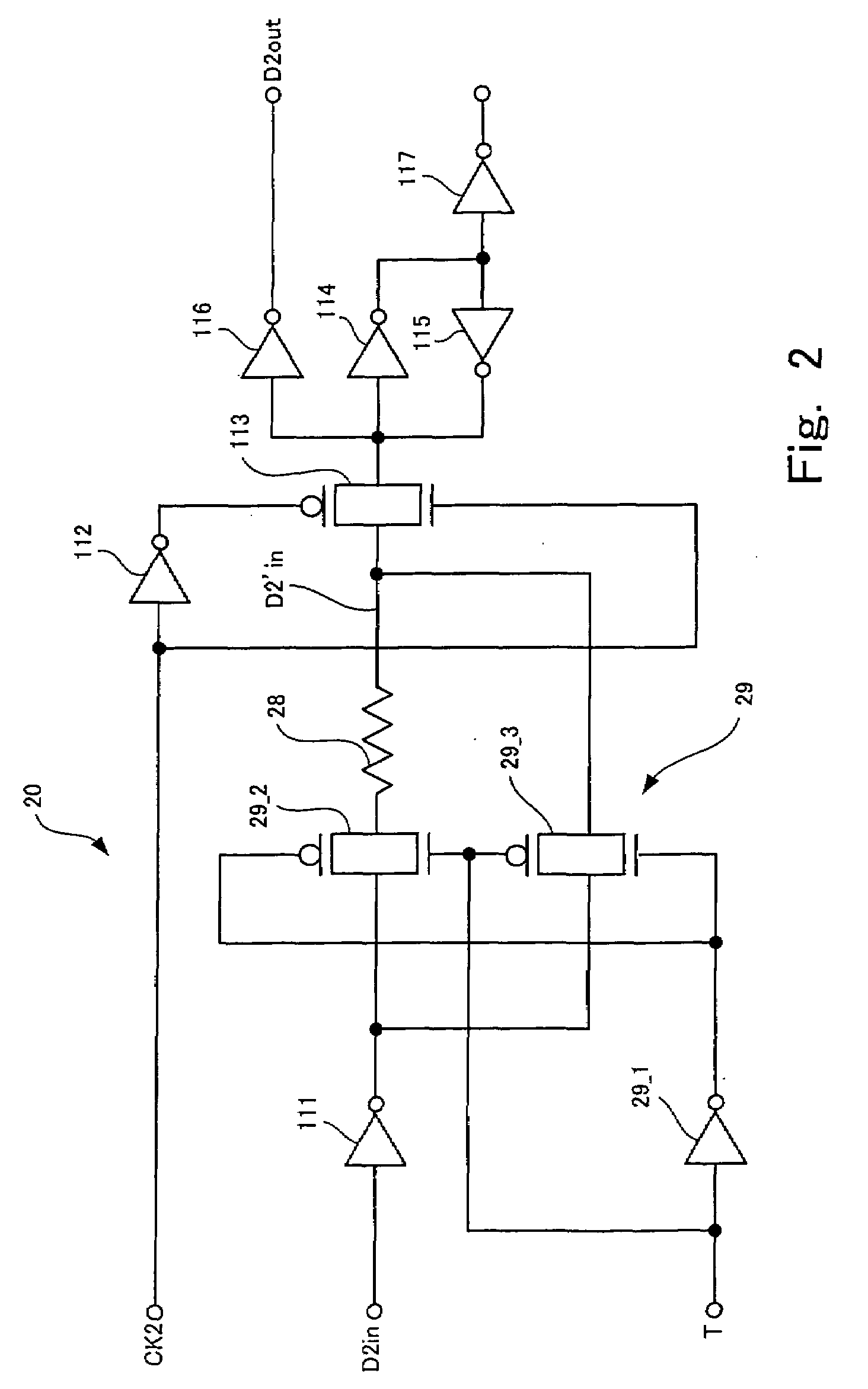
[0054]FIG. 2 is a block diagram showing a circuit structure of a second latch showing in FIG. 1.

[0055]In FIG. 2, the same parts are denoted by the same reference numbers as those of FIG. 10. Only different points will be explained and redundant explanation will be omitted...

second embodiment

[0069]FIG. 4 is a block diagram showing a circuit structure of the second latch that constitutes the first integrated circuit of the present invention.

[0070]According to the embodiment shown in FIG. 4, as compared with the integrated circuit 1 shown in FIG. 1, it is different in the point that the second latch 20 that has the resistive element for the delay of the input signal is replaced by a second latch 40 that has a capacitor for the delay of the input signal.

[0071]According to the second latch 40 shown in FIG. 4, there are provided a transistor 41_1 and a capacitor 41_2, which are connected in series, between the signal input path and the ground.

[0072]The capacitor 41_2 is a delay element for delaying the data D2in transmitted from the first latch 110.

[0073]The transistor 41_1 serves as a path switching circuit for switching the signal input path in such a manner that in the usual operation or the first test, the capacitor 41_2 is bypassed to take the data D2in, and in the seco...


PUM


Abstract

An integrated circuit includes a first latch of a data transmitting source and a second latch of a data receiving destination. The second latch includes: a delay element that delays an input signal transmitted from the first latch; and a path switching circuit that changes over a signal input path in such a way that at time of a usual operation, the input signal is taken through bypassing the delay element and at time of a test operation, the input signal is taken via the delay element.

Description

BACKGROUND OF THE INVENTION[0001]1. Field of the Invention[0002]The present invention relates to an integrated circuit including a first latch of a data transmitting source and a second latch of a data receiving destination.[0003]2. Description of the Related Art[0004]There is a test called WDFT (W (double) clock Dynamic Function Test)) in one of the items that detect the breakdown of the integrated circuit done with LSI tester so far. According to this test, an input signal is entered from the LSI tester to the first latch of the data transmitting source provided in the integrated circuit, and a test is performed whether the second latch of the data receiving destination can take in the input signal transmitted from the first latch. Hereinafter, there will be explained the operation of the first latch in the integrated circuit to which this test is done and the second latch referring to FIG. 9, FIG. 10, and FIG. 11.[0005]FIG. 9 is a block diagram of the conventional integrated circ...

Claims


Application Information

Patent Timeline
IPC IPC(8): H03K3/00
CPCG01R31/31715G01R31/318525G01R31/31725
Inventor OTAKE, TAKASHIKONMOTO, AKIHIKO
Owner FUJITSU LTD
Learn More