
Charged particle beam device and measuring method using the same

a technology of chargeable particles and beams, applied in the direction of electrical equipment, electric discharge tubes, basic electric elements, etc., can solve the problem of reducing measurement accuracy, and achieve the effect of reducing sample damage and reducing measurement accuracy

Active Publication Date: 2016-05-10
HITACHI HIGH-TECH CORP
View PDF7 Cites 3 Cited by
  • Summary
  • Abstract
  • Description
  • Claims
  • Application Information

AI Technical Summary

Benefits of technology

The invention relates to a semiconductor device observation method using an SEM. The technical effects of the invention include reducing damage to the sample by setting low energy of the primary electron beam, improving measurement accuracy by addressing the effect of other optical systems on the electron beam locus, and enhancing sensitivity in observation and measurement of deep grooves and holes by allowing secondary electrons to pass through the energy filter after deflecting them outside the optical axis. The invention also improves the detection of reflected secondary electrons by addressing the limitation of space and a decrease in the number of detected reflected electrons.

Problems solved by technology

However, in a state where the energy of the primary electron beam is low, a locus of the electron beam is subject to an effect of other optical systems (parts), and thus, measurement accuracy is reduced.
However, when the regarding method is used in the SEM disclosed in WO 01 / 075929 A, the following problems occur.

Method used


Image

  • Charged particle beam device and measuring method using the same
  • Charged particle beam device and measuring method using the same
  • Charged particle beam device and measuring method using the same

Examples


first embodiment

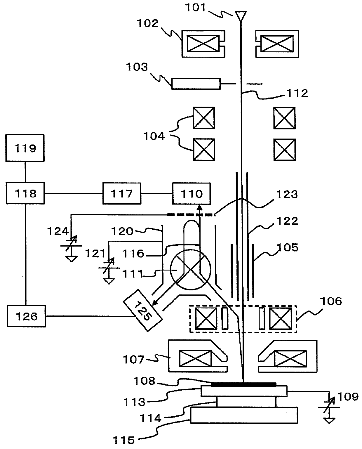
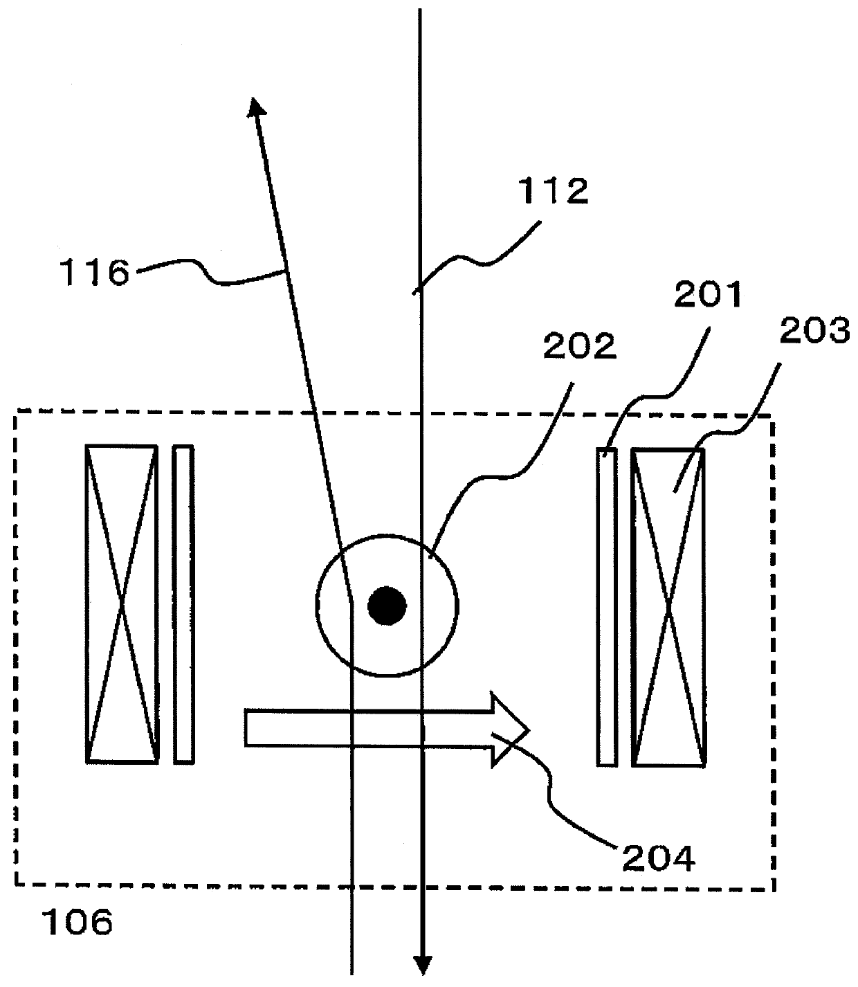
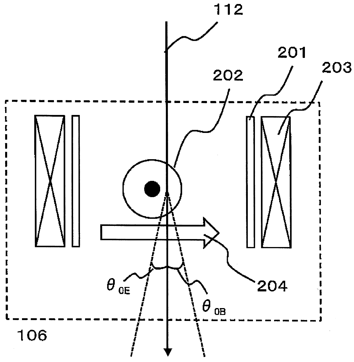
[0050]FIG. 1 is a diagram illustrating a configuration of an SEM according to the present embodiment. In the SEM of FIG. 1, primary electrons 112 generated in an electronic source 101 are condensed by a first condenser lens 102, pass through an aperture 103, are deflected in a deflector 104, pass through an electric field shield 122, pass an ExB deflector 106, are condensed narrow by an object lens 107, and are then incident on sample 108.

[0051]The sample 108 is placed on a sample holder 113, and the sample 108 and the sample holder 113 are electrically contacted. A retarding voltage (VR) can be applied to the sample holder 113 by a retarding power source 109, and the primary electrons 112 are decelerated by the retarding voltage and are incident on the sample 108. Hereinafter, the voltage applied by the retarding power source 109 is VR (<0).

[0052]A sample stage 115 can be moved in an xy plane where an optical axis of the primary electrons 112 is z axis. Further, the sample holder 1...

second embodiment

[0094]A configuration of a second embodiment will be illustrated in FIG. 11. In the present embodiment, an energy filter B1101 and a filter power source B1102 are added to the first embodiment. Here, configurations of the energy filter B1101 and the filter power source B1102 are equal to that of the energy filter A123 and the filter power source A (FIG. 6), and the energy filter B1101 is disposed at the magnetic generator 111 side of the detector B125.

[0095]The first embodiment has a configuration in which the secondary electrons passing through the energy filter A123 and the secondary electrons reflected at the energy filter A123 are respectively detected in the detector A110 and the detector B125. Meanwhile, in the present embodiment, detection of secondary electrons in an arbitrary range, in other words, bandpath detection becomes possible.

[0096]A reason why the bandpath detection becomes possible in the present embodiment will be described with reference to FIG. 12. In the prese...

third embodiment

[0103]FIG. 14 illustrates a configuration of a third embodiment. In the present embodiment, a detector C1401 and an image processor C1402 are added to the configuration of the second embodiment. Note that, in the present embodiment, a secondary electron decelerating electrode 120 has an opening in a direction of the detector C1401.

[0104]In the present embodiment, as the detector C1601, the Everhart-Thornley detector is used, similarly to the detectors A110 and B125. However, the effects of the present embodiment can be obtained even if other electron beam detectors are used for the detector C1601, such as a semiconductor detector or a micro channel plate.

[0105]The method of forming an SEM image in the detector C1601 is similar to the cases of the detectors A110 and B125. That is, the primary electron 112 is deflected by the deflector 104 so that the primary electron 112 scans the sample 108, and a signal detected in the detector C1401 is sent to the image processor C1402. In the ima...


PUM


Abstract

In an SEM provided with an ExB deflector for deflecting secondary electrons outside an optical axis of a primary electron beam between an electronic source and an object lens for condensing the primary electron beam and irradiating a sample with the beam, a unit to decelerate the secondary electrons deflected in the ExB deflector, and a magnetic generator for deflecting the decelerated secondary electron are provided, and a plurality of energy filters and detectors are arranged around the magnetic generator. That is, by separating loci of the secondary electrons incident on the energy filters and of the secondary electrons reflected at the energy filters by the magnetic generator, both of the secondary electrons are concurrently detected.

Description

CROSS-REFERENCE TO RELATED APPLICATION[0001]This application claims the priority of Japanese Patent Application No. 2013-077335 filed Apr. 3, 2013, which is incorporated herein by reference in its entirety.BACKGROUND OF THE INVENTION[0002]1. Field of the Invention[0003]The present invention relates to a charged particle beam device, and a measuring method using the same.[0004]2. Description of the Related Art[0005]Currently, in the manufacturing line of semiconductors, technologies of measuring the dimension of a circuit pattern formed on a wafer in the middle of a process have a significant role for improvement of the yield. Conventionally, most of the measuring technologies have been based on optical microscopes. However, currently, measuring devices based on SEMs (hereinafter, SEM-based length measuring devices) have been widely spread due to micronization of semiconductor patterns.[0006]Then, in recent years, diversification and three dimensional structures of materials used in ...

Claims


Application Information

Patent Timeline
Patent Type & Authority Patents(United States)
IPC IPC(8): H01J37/00H01J37/244H01J37/28
CPCH01J37/28H01J37/244H01J2237/2448H01J2237/2449H01J2237/24485H01J2237/281H01J2237/2806
Inventor BIZEN, DAISUKEKAWANO, HAJIMEKAZUMI, HIDEYUKI
Owner HITACHI HIGH-TECH CORP
Learn More