[0027]The data IO portion may include a plurality of data input portions for receiving the test pattern data from the external portion and applying the test pattern data to the data IO control portion, and a plurality of data output portions for receiving the test pattern data output from the data IO control portion and conditionally outputting the test pattern data as the test status data in response to the output control signal. Each of the data output portions may include a tri-state buffer, which conditionally outputs the test pattern data as the test status data in response to the output control signal.
[0028]The data IO portion may include a plurality of data input portions for receiving the test pattern data from the external portion and applying the test pattern data to the data IO control portion, and a plurality of data output portions for receiving the test pattern data output from the data IO control portion, and conditionally inverting and outputting the test pattern data as the test status data in response to the output control signal. Each of the data output portions may include a first switch for conditionally outputting the test pattern data as the test status data to the external portion in response to the output control signal, an inverter for inverting the test pattern data, and a second switch for conditionally outputting the inverted test pattern data as the test status data to the external portion in response to the output control signal, which conditionally blocks the test pattern data output as the test status data.
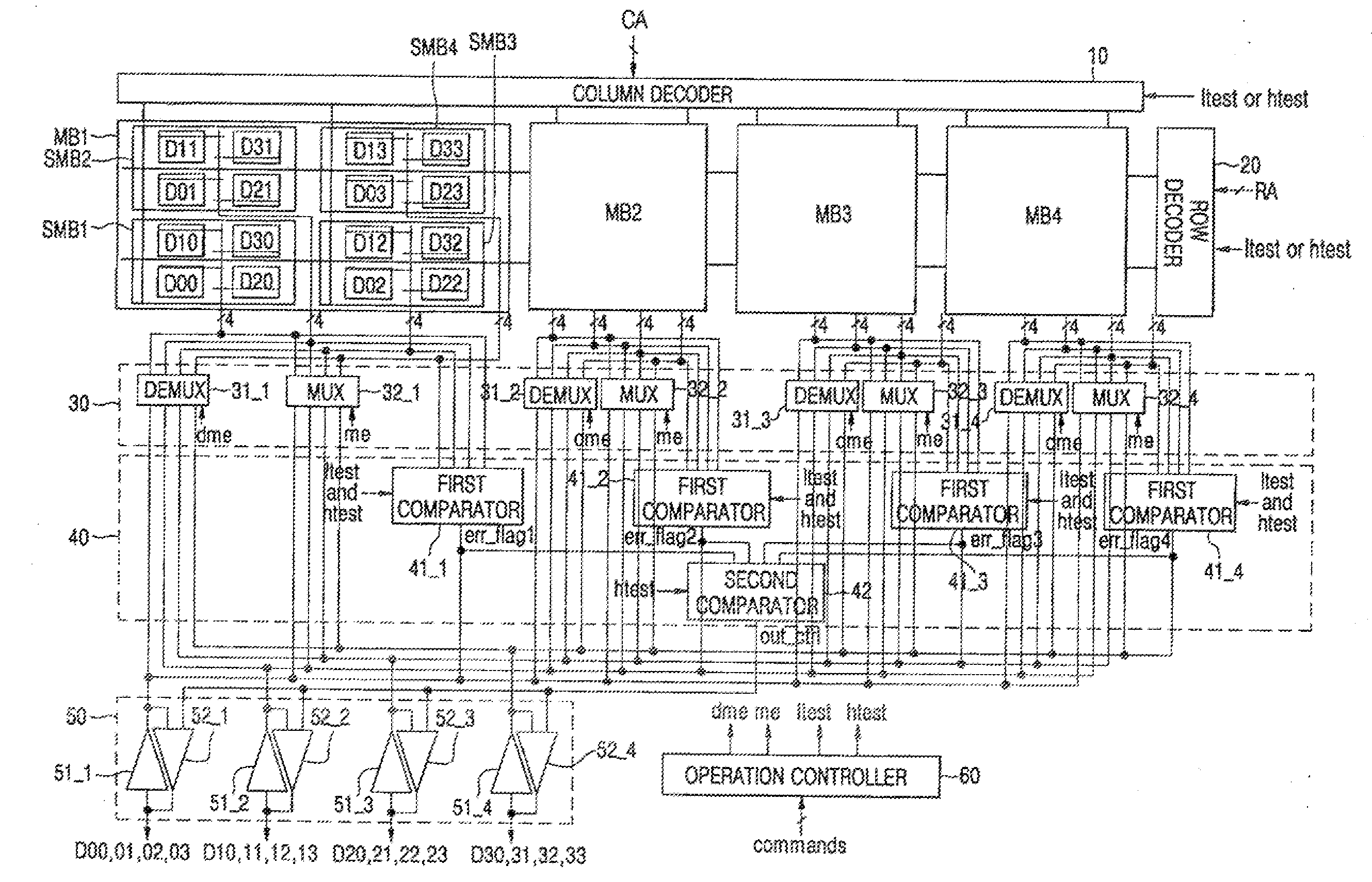
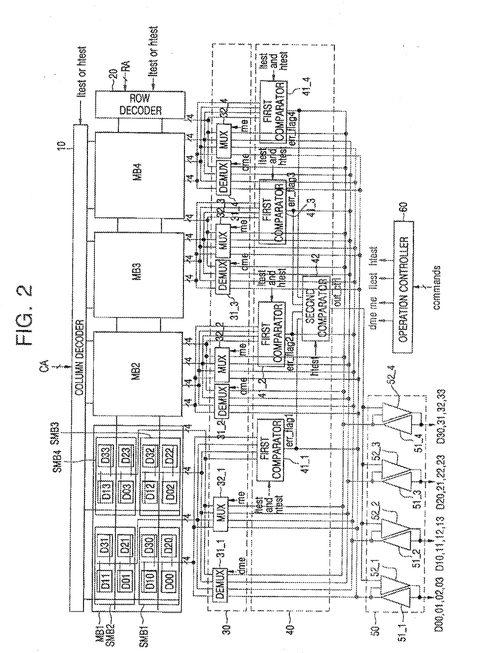
[0029]An embodiment of the present invention includes a semiconductor memory device comprising a memory cell array including a plurality of memory regions, an address decoding portion for decoding an address applied from an external portion for simultaneously selecting all of the plurality of memory regions during first and second test read operations, a data IO control portion for receiving test pattern data and writing the test pattern data to each of the plurality of memory regions during a first write operation, stopping its operation during the first read operation, and reading the test pattern data from one of the plurality of memory regions and outputting the test pattern data during the second test read operation, a data IO portion for receiving the test pattern data from the external portion and applying the test pattern data to the data IO control portion during the first and second test write operations, outputting error detecting signals as test status data to the external portion during the first test read operation, and receiving the test pattern data output from the data IO control portion and conditionally outputting the test pattern data as the test status data to the external portion in response to an output control signal during the second test read operation, and a test control signal generating portion for comparing the test pattern data read from the plurality of memory regions to generate the error detecting signals for indicating an error occurrence and comparing the error detecting signals to generate an output control signal for conditionally outputting the test pattern data as the test status data, wherein the error detecting signals are output to the data IO portion during the first test read operation and the output control signal is output to the data IO portion during the second test read operation.
[0030]Each test pattern data may have the same data value. The test control signal generating portion may include a plurality of first comparators, which correspond to the plurality of memory regions, to determine whether the test pattern data output from the corresponding memory regions are identical, to generate error detecting signals for indicating an error occurrence and to apply the error detecting signals to the data IO portion during the first test read operation, and a second comparator for receiving the error detecting signals of the first comparators, generating the output control signal, which allows the test pattern data output as the test status data when all of the error detecting signals indicate no error occurrence and blocks the test pattern data output as the test status data when one or more of the error detecting signals indicate an error occurrence, and applying the output control signal to the data IO portion during the second test read operation.
[0031]The data IO portion may include a plurality of data input portions for receiving the test pattern data from the external portion and applying the test pattern data to the data IO control portion, and a plurality of data output portions for receiving the error detecting signals from the test control signal generating portion and conditionally outputting the test pattern data as the test status data to the external portion during the first read operation, receiving the test pattern data from the data IO control portion dining the second test read operation, and conditionally outputting the test pattern data as the test status data to the external portion in response to the output control signal. Each of the data output portions may include a tri-state buffer which conditionally outputs the test pattern data as the test status data in response to the output control signal.
[0032]The data IO portion may include a plurality of data input portions for receiving the test pattern data from the external portion and applying the test pattern data to the data IO control portion, and a plurality of data output portions for receiving the error detecting signals from the test control signal generating portion and outputting the error detecting signals during the first read operation, and receiving the test pattern data from the data IO control portion and conditionally inverting and outputting the test pattern data as the test status data in response to the output control signal during the second test read operation. Each of the data output portions may include a first switch for conditionally outputting tire test pattern data as the test status data to the external portion in response to the output control signal, an inverter for inverting the test pattern data, and a second switch for conditionally outputting the inverted test pattern data as the test status data to the external portion in response to the output control signal, which conditionally blocks the test pattern data output as the test status data.

