
Switching device

a technology of switching device and voltage source, which is applied in the direction of electronic switching, two-wire dc circuit, pulse technique, etc., can solve the problems of switching control not being able to be done between the above voltages vddb>, source on the interrupted side becoming conductive, etc., and achieve the effect of reducing the mounting scale of input/output processing device which individually required different voltage sources

Inactive Publication Date: 2008-02-28
PANASONIC SEMICON SOLUTIONS CO LTD
View PDF4 Cites 28 Cited by
  • Summary
  • Abstract
  • Description
  • Claims
  • Application Information

AI Technical Summary

Benefits of technology

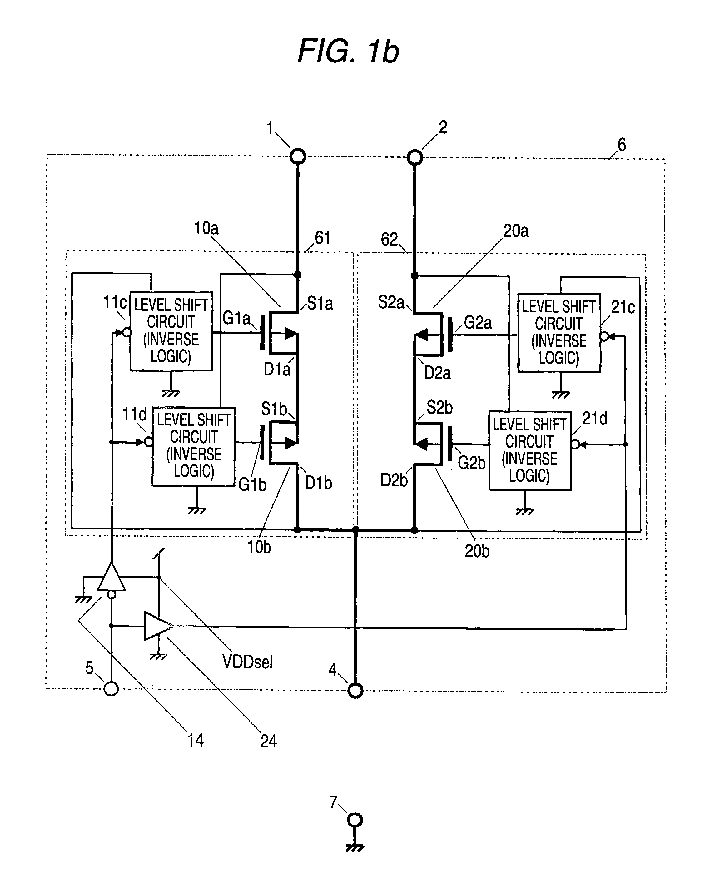
[0028] The switching device according to this invention, firstly, employs enhancement type PMOS transistors (first means) as a means for effectively selecting conduction or interruption between a voltage source and its power-supplied device.
[0047] Secondly, where there are a plurality of signal input / output processing devices which are used exclusively from one another and require different voltage source voltages, and they are replaced by another processing device in which the common functions of the input / output processing devices are unified with the terminals thereof, one of voltage sources for another processing device can be switch-selected by the switching device according to this invention. In this way, the mounting scale of the input / output processing devices which individually required different voltage sources can be reduced.

Problems solved by technology

This embodiment presented a problem that unless a voltage source voltage VDDsel of a switching control logic inverter is kept so as to be not lower than a voltage source voltage VDD1 or VDD2, the voltage source on the interrupted side becomes conductive.
However, switch control could not be done between the above voltages VDD1 and VDD2.
This embodiment presents a problem that if the difference between two voltage source voltages exceeds the forward diode voltage of a parasitic diode that is necessarily generated at the interface between the P-channel electrode and N-well of each of enhancement type PMOS transistors T1 and T3, the voltage source on the interrupted side becomes conductive.

Method used


Image

  • Switching device
  • Switching device
  • Switching device

Examples


embodiment i

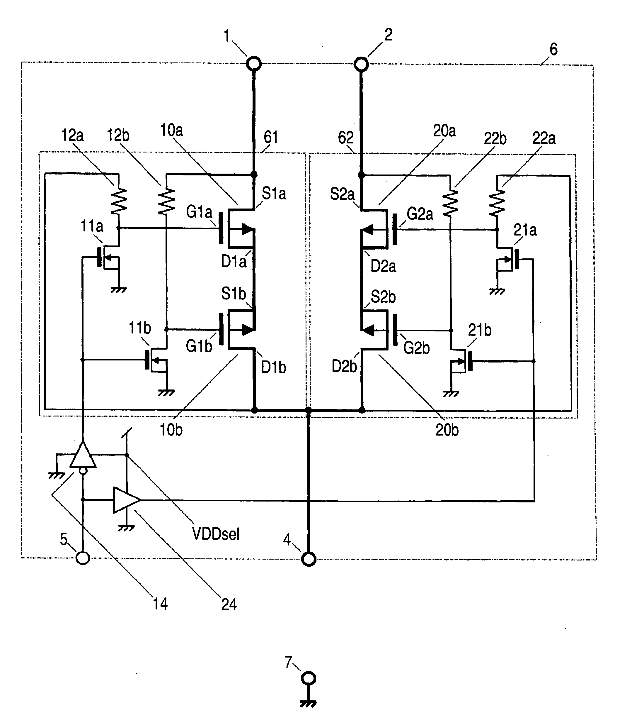
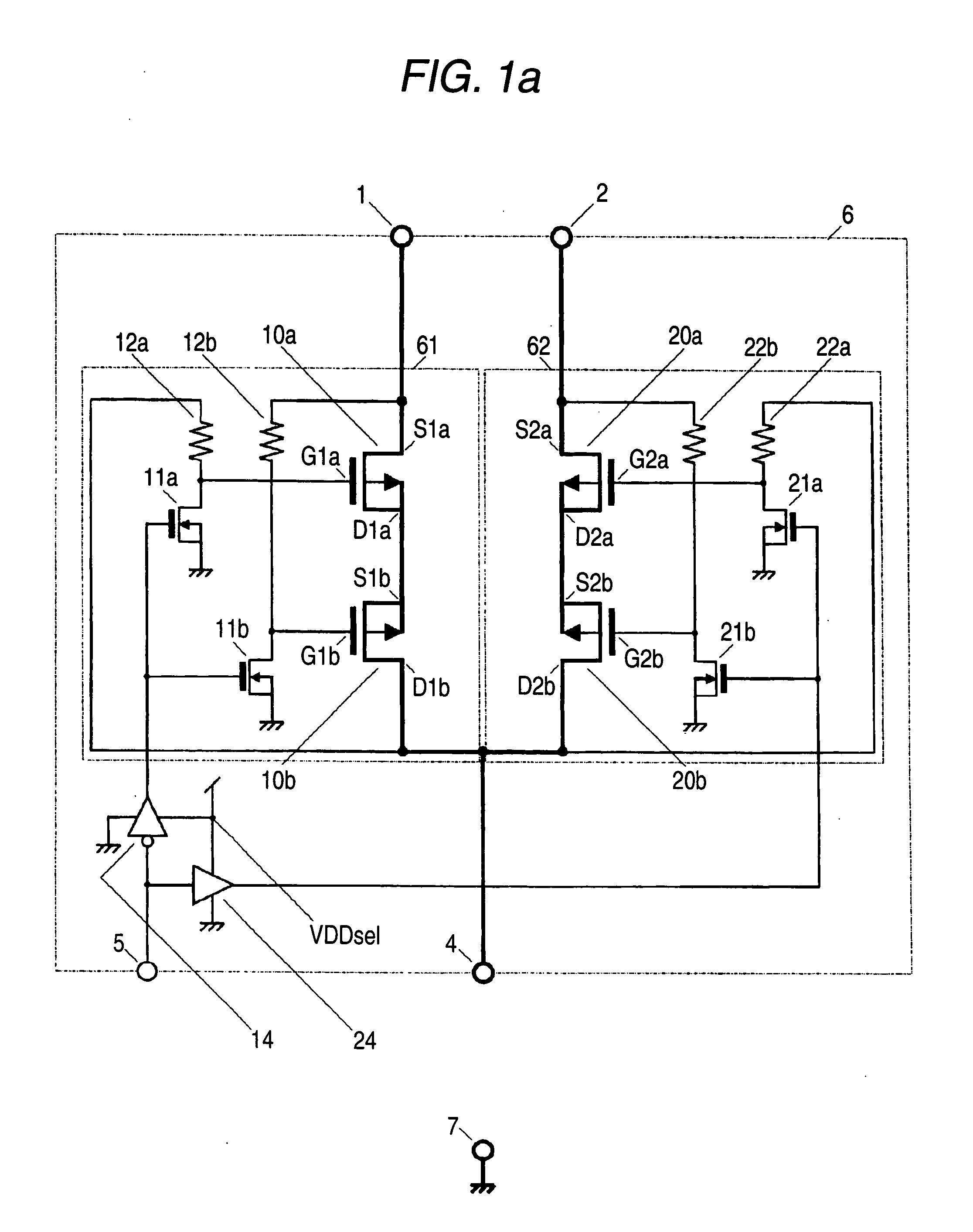
[0063]FIG. 1a shows an embodiment I that includes the first to third means for solving the problems. In FIG. 1a, a voltage source switching device 6 includes voltage source input terminals 1 and 2 for connection to voltage sources, an voltage source output terminal 4 for connection to a power-supplied device for the voltage sources, a voltage source switching path 61 between the input terminal 1 and output terminal 4, a voltage switching path 62 between the input terminal 2 and output terminal 4, and a switch-controlling circuit composed of a logic inverter 14 and a logic inverter 24 having a switch-controlling input terminal 5 for switch-selecting either one of these input terminal 1 or 2 to the output terminal 4.

[0064] The above switching path 61 includes, between the input terminal 1 and the output terminal 4 for the corresponding voltage source, a series connection of a source electrode or a drain electrode of PMOS transistors 10a and 10b (first and second PMOS transistors), an...

embodiment ii

[0105]FIG. 8 shows Embodiment II related to the above Embodiment I. In FIG. 8, immediately after the switching control logic inverter 14 and logic buffer 24 in FIG. 1a, logic input rising delay circuits 15 and 25 are inserted, each of which gives a rising delay only when the logic input is supplied to the logic inverter 14 and logic buffer 25, and delays the conducting timing of the voltage source for the interrupting timing thereof.

[0106] In order to solve the problem of Embodiment I shown in FIG. 1a, the above configuration intends to prevent occurrence of a moment when the PMOS transistors 10a, 10b, 20a, 20b are simultaneously and instantaneously conducted when the voltage source is switched from the voltage source input terminal 1 to 2, or from 2 to 1.

[0107] This inconvenience is attributable to the fact that the time taken for the PMOS transistor on the conducted side of the voltage source to shift from its saturated state filled with electrons in its P-channel to its interru...

embodiment iii

[0113] Embodiment III which is an application of Embodiments I and II is shown in FIG. 10(b). FIG. 10(a) shows a conventional example corresponding to FIG. 10(b). In FIG. 10(a), one of signal input / output processing devices 91, 92, 93 requiring different voltage source voltages is exclusively switch-connected to a signal input / output terminal 9 common to them by a switching control input terminal 5.

[0114] The above processing devices 91, 92, 93, which generally have different voltage amplitude specifications for the signal input / output terminal 9, required different voltage source input terminals 1, 2, 3. Therefore, even if a part of the processing devices are unified as long as the voltage source voltages are common, since these voltage source voltages are different, the processing devices 91, 92, 93 must be given an overlapped function, respectively. As a result, as the case may be, the entire mounting apparatus shown in FIG. 10(a) was upsized.

[0115] In FIG. 10(b), between the v...


PUM


Abstract

To provide a switching device capable of a switch-controlling a voltage source regardless of voltage changes in the voltage source to be switched and the voltage source employed for switch control. A switching path 61 includes, between the input terminal 1 and output terminal 4 for a voltage source, a series connection of the source or drain electrodes of PMOS transistors 10a and 10b connected to their back-gate electrode. A driving circuit has an NMOS transistor 11a having a load resistor 12a at its drain electrode and NMOS transistor 11b having a load resistor 12b at its drain electrode, which are connected to the gate electrodes of the PMOS transistors, respectively and receives the output from the logic inverter 14 for the switching control.

Description

BACKGROUND OF THE INVENTION [0001] 1. Field of the Invention [0002] This invention relates to a switching device for select-switching the connection between a voltage source and a power-supplied device. [0003] 2. Description of the Related Art [0004] As a conventional means for selectively switching an any source from a plurality of voltage sources in an individual semiconductor device or integrated circuit, where one of two kinds of input voltages having different magnitudes is selected as an output voltage, there is a previously known supplied voltage switching circuit in which even if the voltage applied to a first input terminal becomes lower than the voltage applied to a second input terminal, an overcurrent is prevented from passing through a transistor internally provided (for example, see Patent Reference 1). [0005] Further, like PROM, where a plurality of power sources having different voltage levels in operation are used by switching inside a semiconductor device, there is...

Claims


Application Information

Patent Timeline
Patent Type & Authority Applications(United States)
IPC IPC(8): H02J3/00
CPCH02J1/06H02J2001/008H03K17/063H03K17/161H03K17/693H03K17/302H03K17/6871H03K17/6872H03K17/28H02J1/082
Inventor KIHARA, HIDEYUKINAGUMO, KATSUMI
Owner PANASONIC SEMICON SOLUTIONS CO LTD
Learn More