Touch screen devices employing nanostructure networks

a nanostructure network and touch screen technology, applied in the field of touch screen display, can solve the problems of 75% clarity, the indium component of ito is rapidly becoming a scarce commodity, and the transparent layer can be easily damaged by sharp objects

Inactive Publication Date: 2008-02-28
UNIDYM
View PDF3 Cites 146 Cited by
  • Summary
  • Abstract
  • Description
  • Claims
  • Application Information

AI Technical Summary

Benefits of technology

[0017]Methods of fabricating the above-mentioned and other embodiments of the present invention comprise depositing first a network of nanostructures on a transparent substrate, wherein the network of nanostructures forms a conductive layer. Such methods may further comprise depositing a spacer layer on the conductive layer and affixing it to a second coated transparent substrate such that the conductive layers face each other and the spacer layer

Problems solved by technology

Resistive touch screen displays are generally the most affordable, but offer only 75% clarity and the transparent layer can be easily damaged by sharp objects.
However, ITO can be an

Method used


Image

  • Touch screen devices employing nanostructure networks
  • Touch screen devices employing nanostructure networks
  • Touch screen devices employing nanostructure networks

Examples


Embodiment Construction

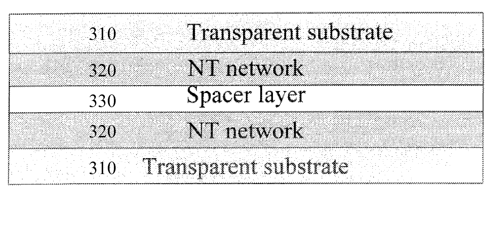
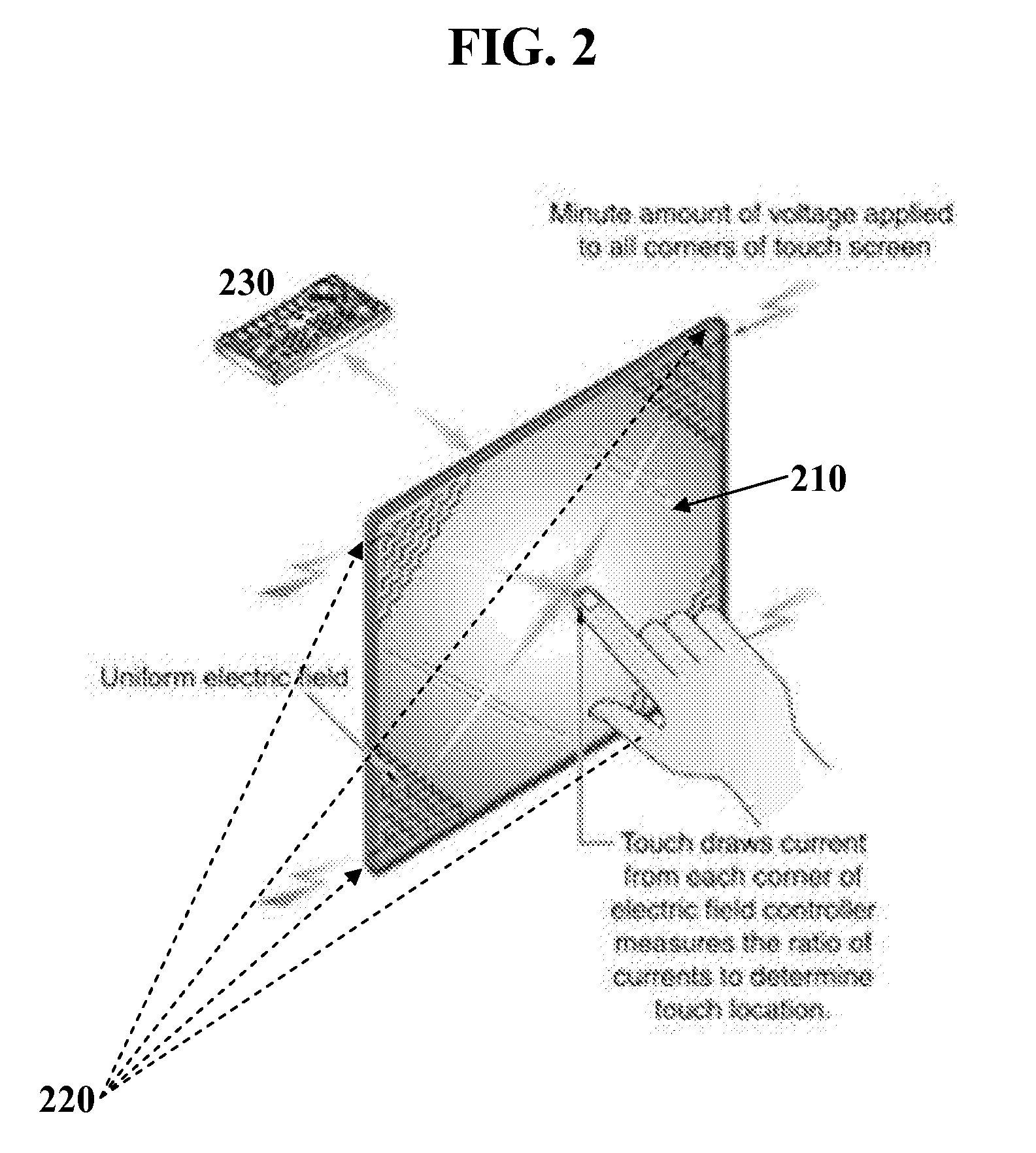
[0029]Referring to FIG. 1, a resistive touch screen display comprises a transparent substrate 160 (e.g., plastic or glass) covered with two transparent conductive layers 140 separated by an array of insulating spacers 150. The top transparent conductive layer is often covered by an anti-Newton ring coating 130 (e.g., acrylic with Silica) and packaged with a transparent plastic layer 120 (e.g., PET) and hardcoat 110.

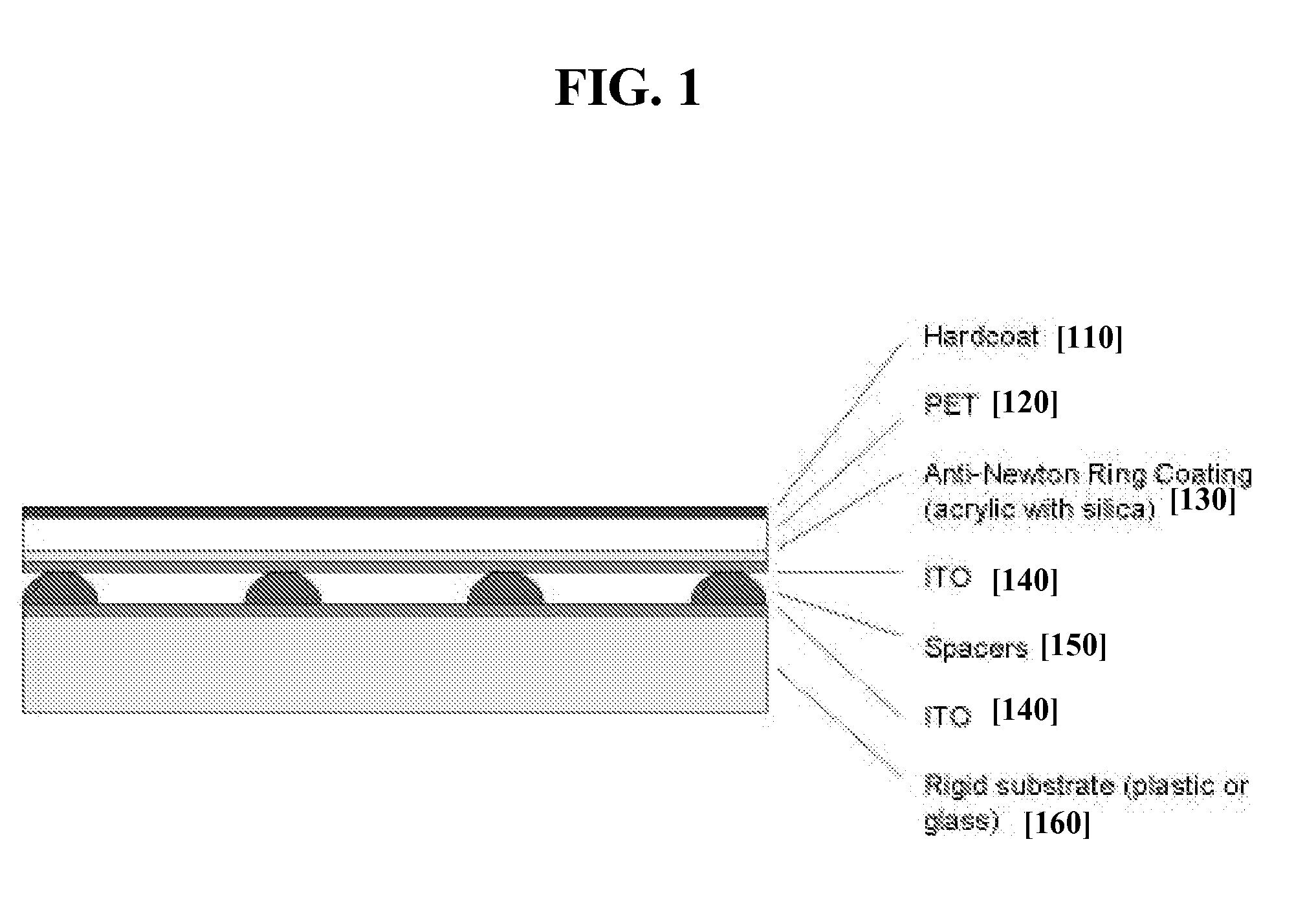
[0030]While the display is operational, an electrical current runs through the two transparent conductive layers 140. When a user touches the display, e.g., by pushing down on the hardcoat, the layers above the spacers deform and the two transparent conductive layers 140 make contact at an underlying point. The resulting change in the electrical field at that point is detected and the coordinates of the point are calculated by a computer.

[0031]Although the transparent conductive layers most commonly consist of Indium-tin-oxide (ITO), ITO is relatively brittle and is there...


PUM


Abstract

Touch screen displays comprising at least one nanostructure-film, and fabrication methods thereof, are discussed. Nanostructure-films may comprise, for example, a network(s) of nanotubes, nanowires, nanoparticles and/or graphene flakes. Such films are preferably at least semi-transparent and relatively flexible, making them well-suited for use in a variety of touch screen applications.

Description

[0001]This application claims priority to U.S. Provisional Patent Application No. 60 / 836,966, filed Aug. 11, 2006, and entitled “FABRICATION OF LARGE AREA HIGHLY CONDUCTING NANOSTRUCTURE FILMS,” which is hereby incorporated herein by reference.COPYRIGHT & TRADEMARK NOTICE[0002]A portion of the disclosure of this patent document contains material that is subject to copyright protection. The owner has no objection to the facsimile reproduction by any one of the patent document or the patent disclosure, as it appears in the Patent and Trademark Office patent file or records, but otherwise reserves all copyrights whatsoever.[0003]Certain marks referenced herein may be common law or registered trademarks of third parties affiliated or unaffiliated with the applicant or the assignee. Use of these marks is by way of example and shall not be construed as descriptive or limit the scope of this invention to material associated only with such marks.FIELD OF THE INVENTION[0004]The present inven...

Claims


Application Information

Patent Timeline
IPC IPC(8): G06F3/045
CPCG06F3/045G06F3/044G06F3/0445
Inventor HU, LIANGBINGGRUNER, GEORGE
Owner UNIDYM
Why Eureka
Try Eureka