Output circuit of semiconductor device

a technology of output circuit and semiconductor device, which is applied in the direction of digital storage, pulse technique, and increase in reliability modifications, can solve the problems of large error of output impedance along the increase in the number of unit buffers used in parallel, and achieve the effect of increasing the data transfer speed of the system and facilitating higher-speed data processing systems

Active Publication Date: 2008-03-06
LONGITUDE LICENSING LTD
View PDF10 Cites 36 Cited by
  • Summary
  • Abstract
  • Description
  • Claims
  • Application Information

AI Technical Summary

Benefits of technology

[0022]As explained above, according to the present invention, because the resistance values of resistors included in the unit buffers are differentiated, the deviation of impedances attributable to the power source resistance can be offset. Therefore, even when the number of unit buffers used in parallel is large, the impedance of the output circuit can be set to approximately a desired value.
[0023]Further, by carrying out the accurate calibration operation, the data transfer speed on the system can be increased, and a higher-speed data processing system can be configured.

Problems solved by technology

However, as a result of researches the present inventors have carried out about the method of using unit buffers in parallel, it has become clear that the error of the output impedance becomes large along the increase in the number of unit buffers used in parallel.
As a result, the present inventors have found that a power source resistance present between the power source terminal and the output circuit is a main cause of the increase in errors.

Method used


Image

  • Output circuit of semiconductor device
  • Output circuit of semiconductor device
  • Output circuit of semiconductor device

Examples


first embodiment

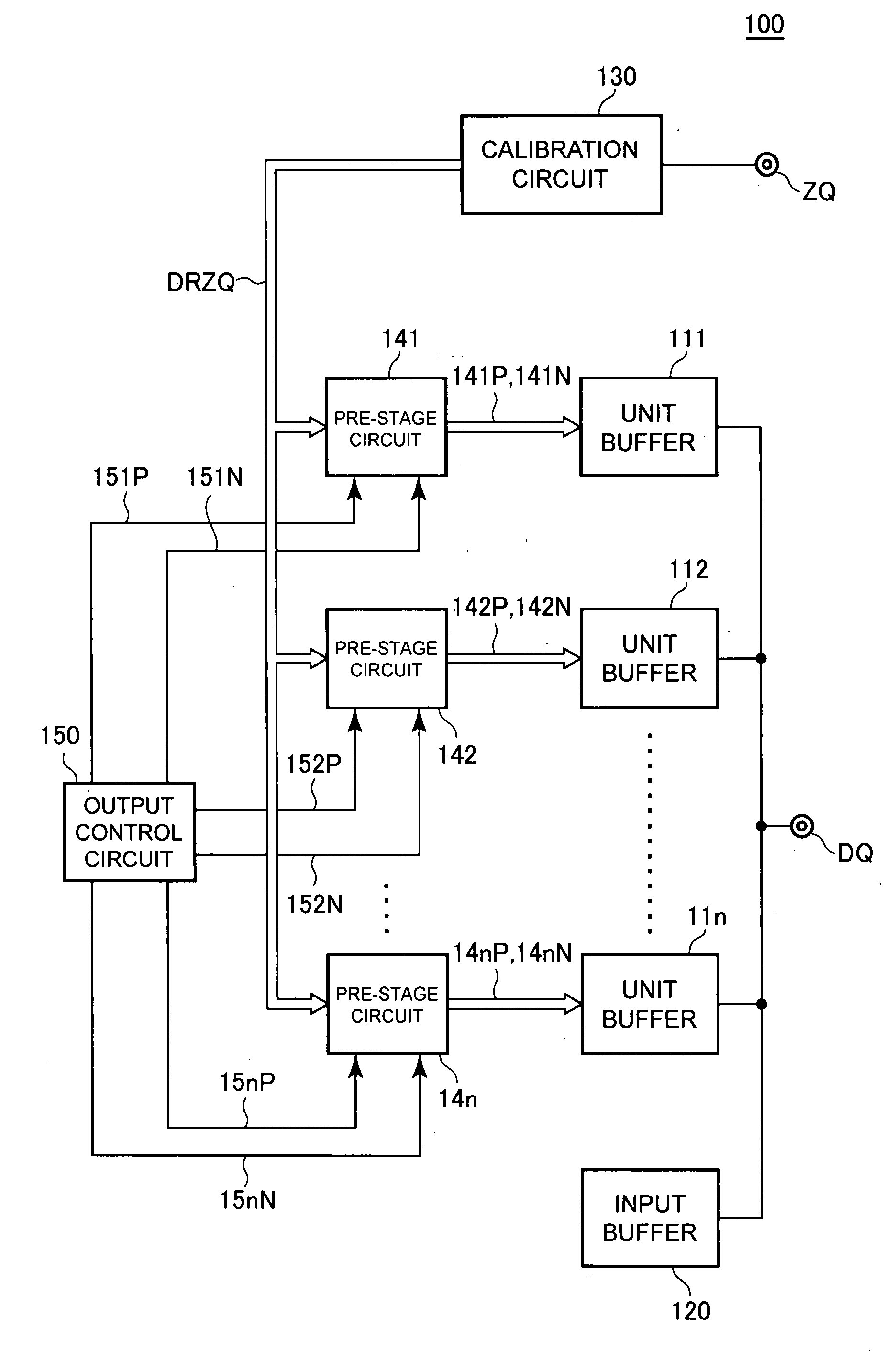
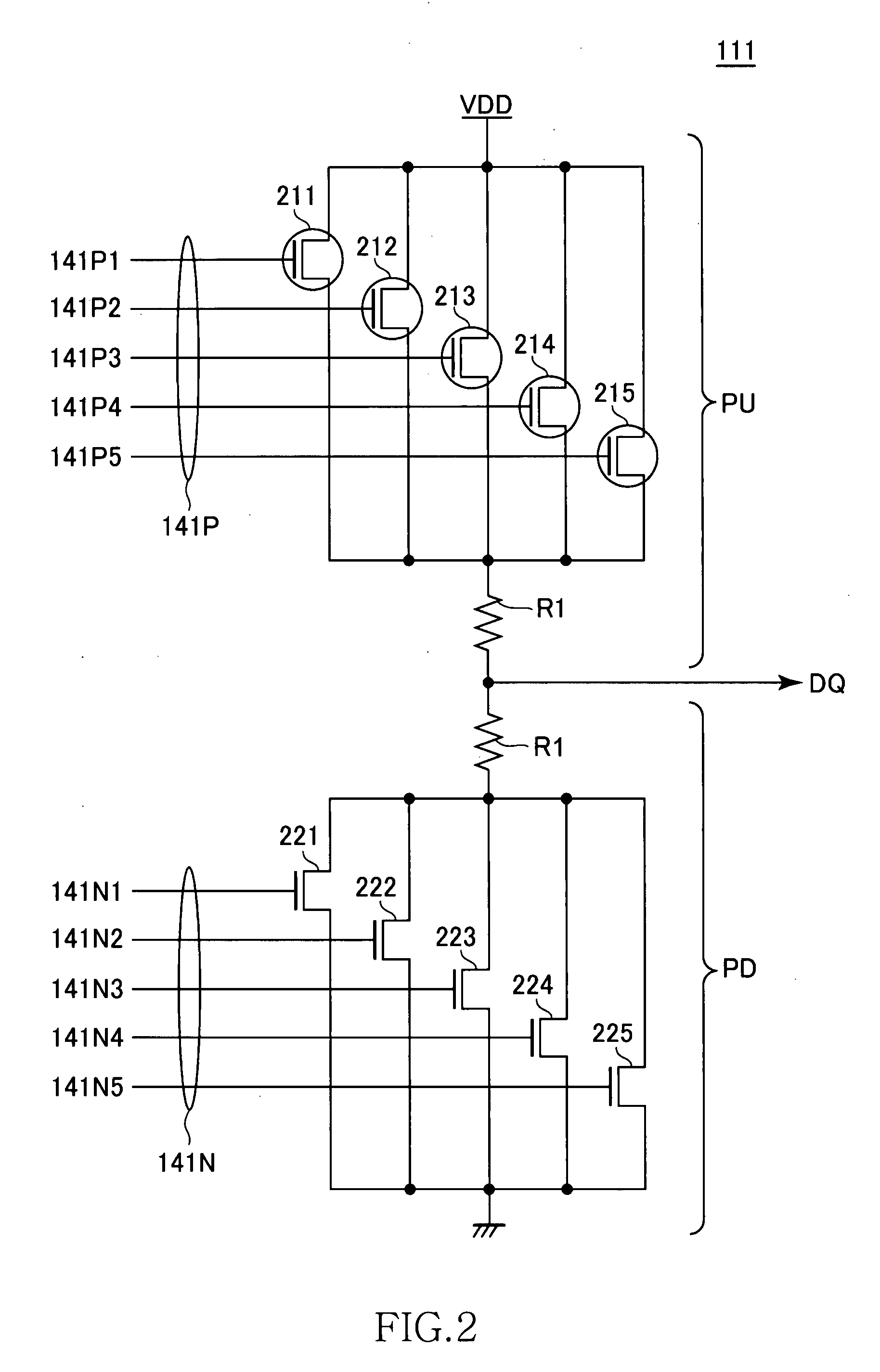
[0139]For example, in the first embodiment, as shown in FIG. 3, the resistors R1 to Rn are inserted into between the transistors 111P to 11nP at the pull-up side and the output terminal DQ and into between the transistors 111N to 11nN at the pull-down side and the output terminal DQ, and the resistance values of the resistors R1 to Rn are differentiated from one another. However, the present invention is not limited to this. As shown in FIG. 16, the resistors between these transistors and the output terminal DQ can be consistently set to Rn, and separate resistors R11, R12, . . . can be set between the transistors and the power source terminal VDDQ and the power source terminal VSSQ.

[0140]In this case, when the relationships of Rn+R11=R1, Rn+R12=R2, . . . are satisfied by setting the resistance values of the resistors R11, R12, . . . as R11>R12>, . . . , the same effect as that of the first embodiment can be obtained. According to this method, the resistors between the transistors a...

second embodiment

[0141]In the second embodiment, each of the two unit buffers 521 and 522 that constitute the output buffer 520 has an independent circuit. Similarly, each of the three unit buffers 531 to 533 that constitute the output buffer 530 also has an independent circuit. However, these circuits do not need to be completely independent of each other. So long as individual unit buffers can be regarded as the same as a replica buffer, these unit buffers can be mutually connected within the output buffer, as shown in FIG. 17.

[0142]FIG. 17 shows the three unit buffers 531 to 533 that constitute the output buffer 530, and that are connected to each other inside the output buffer 530. In this example, the contacts of the P-channel MOS transistor that is included in the pull-up circuit PU and the resistor are connected to each other. Similarly, the contacts of the N-channel MOS transistor that is included in the pull-down circuit PD and the resistor are connected to each other. In this case, the ind...


PUM


Abstract

An output circuit of a semiconductor includes unit buffers, each unit buffer having transistors and resistors connected between a power source terminal VDDQ and an output terminal DQ, and transistors and resistors connected between a power source terminal VSSQ and an output terminal DQ. On-resistance values of transistors included in the unit buffers are mutually substantially the same, and resistance values of resistors included in the unit buffers are mutually different. A deviation of impedances attributable to a power source resistance can be offset based on a difference between resistance values of the resistors.

Description

TECHNICAL FIELD[0001]The present invention relates to an output circuit of a semiconductor device. Particularly, the invention relates to an output circuit capable of changing over an output impedance. The present invention also relates to a data processing system that includes a semiconductor memory device having an output circuit.BACKGROUND OF THE INVENTION[0002]In recent years, significantly high data transfer rate is required for data transfer between semiconductor devices (between CPUs and memories for example). To accomplish high data transfer rate, the amplitude of input / output signals is increasingly reduced. If the input / output signals have reduced amplitudes, the desired accuracy of impedances of output buffers becomes severe.[0003]The impedance of the output buffer varies depending on process conditions during the manufacturing. Also, during its actual use, the impedance of the output buffer is affected by variations in ambient temperature and power source voltage. When h...

Claims


Application Information

Patent Timeline
Patent Type & Authority Applications(United States)
IPC IPC(8): H03K17/16
CPCG11C7/1051G11C7/1057H03K19/018571H03K17/6872H03K19/0005G11C2207/2254
Inventor KINOSHITA, HIROTOFUJISAWA, HIROKI
Owner LONGITUDE LICENSING LTD
Why Eureka
Try Eureka