Method for characterizing line width roughness (LWR) of printed features

a technology of printed features and roughness, which is applied in the field of non-destructive methods for measuring and characterizing line width roughness (lwr) of printed features, can solve the problems of undesirable electric charging of dielectric materials, loss of definition of lines, and damage to the 193-nm photoresist pattern

Inactive Publication Date: 2008-03-06
UNITED MICROELECTRONICS CORP
View PDF4 Cites 26 Cited by
  • Summary
  • Abstract
  • Description
  • Claims
  • Application Information

AI Technical Summary

Benefits of technology

[0008]It is one object of the present invention to provide a non-destructive method for measuring and assessing line width roughness (LWR) of a printed feature by utilizing an optical CD metrology tool in order to solve the above-mentioned problems.

Problems solved by technology

Because critical dimensions (CDs) shrink by one-half every six years, lines tend to lose definition, which makes them rougher.
LER, which is a persistent problem for 193-nm lithography, refers to the variations on the sidewalls of patterned features or random fluctuations in the width of a resist feature.
However, the conventional CD-SEM imaging technology is destructive and may result in damage to the 193-nm photoresist pattern and undesirable electric charging on the dielectric materials.

Method used


Image

  • Method for characterizing line width roughness (LWR) of printed features
  • Method for characterizing line width roughness (LWR) of printed features
  • Method for characterizing line width roughness (LWR) of printed features

Examples


Embodiment Construction

[0016]Smaller device and dimensions and tighter process control windows have created a need for CD metrology tools having higher levels of precision and accuracy. As critical dimensions (CD) for semiconductor devices shrink to a few tens of nanometers, the line edge roughness (LER) and line width roughness (LWR) becomes a critical issue.

[0017]As previously described, LER of a patterned line is an accumulation of the roughness originating from the resist, materials and etch. At the 90-nm and below, controlling the cross-sectional profile of critical layer structures such as gate patterning is key to maximizing yield and transistor performance.

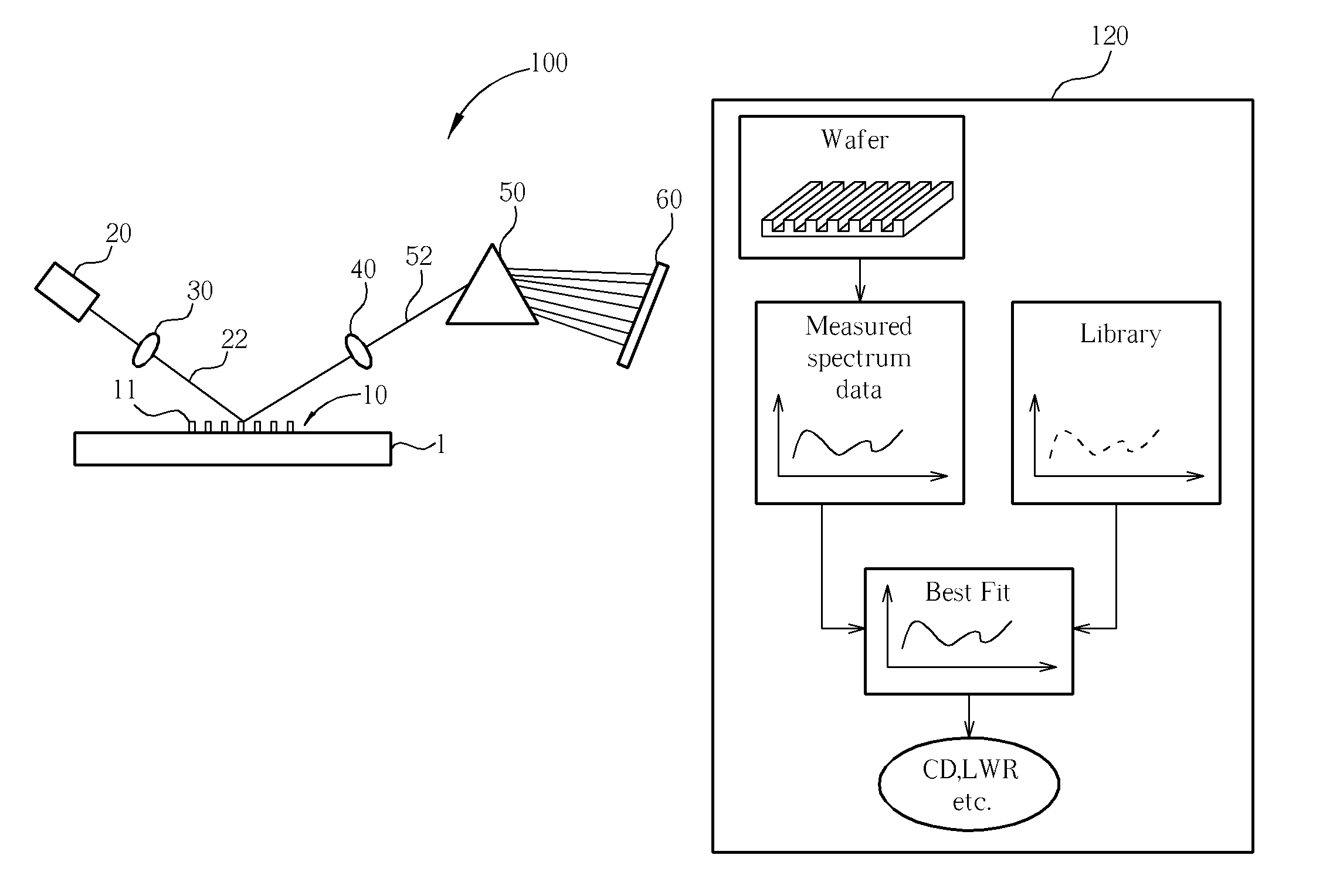
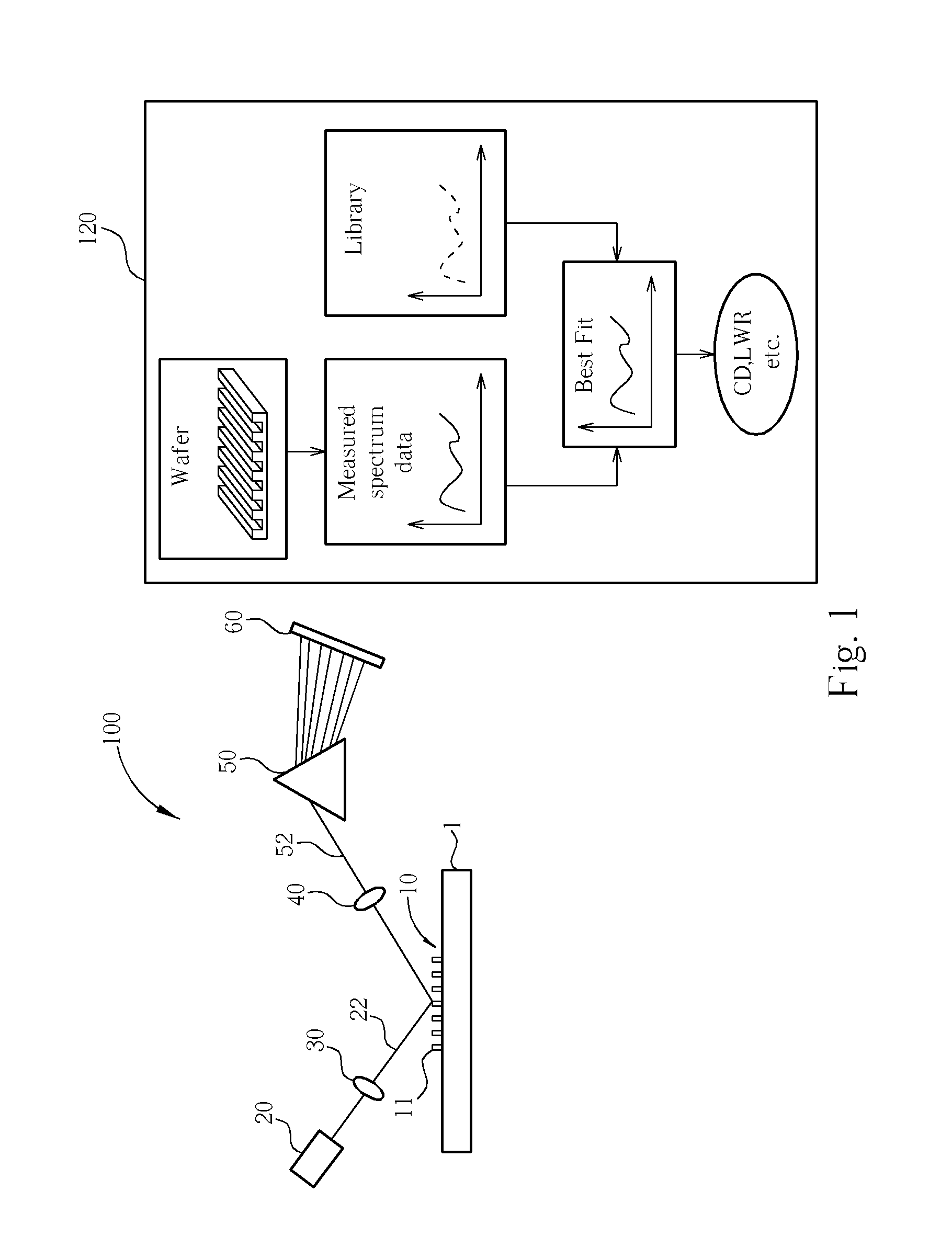
[0018]The present invention pertains to a non-destructive, optical method for measuring and characterizing line width roughness (LWR) of a printed feature such as a critical layer of resist lines, which provides chipmakers with an effective in-line process control. The non-destructive, optical method of this invention is implemented using a spec...


PUM


Abstract

A method for characterizing line width roughness of printed features is provided. A wafer having thereon a plurality of gratings formed within a test key region is prepared. The wafer is transferred to a spectroscopic ellipsometry tool having a light source, a detector and a computer. A polarized light beam emanated from the light source is directed onto the gratings. Spectrum data of reflected light is measured and recorded. The spectrum data is compared to a library linked to the computer in real time. The library contains a plurality of contact-hole model based spectra created by incorporating parameter values that describes the line width roughness. The spectrum data is matched with the contact-hole model based spectra, thereby determining the parameter values.

Description

BACKGROUND OF THE INVENTION[0001]1. Field of the Invention[0002]The present invention relates generally to the fabrication of semiconductor devices and, more particularly, the present invention relates to a non-destructive method for measuring and characterizing line width roughness (LWR) of a printed feature.[0003]2. Description of the Prior Art[0004]In the semiconductor industry, there is a continuing trend toward higher device densities. To achieve these high densities there has been and continues to be efforts toward scaling down the device dimensions on semiconductor wafers. Because critical dimensions (CDs) shrink by one-half every six years, lines tend to lose definition, which makes them rougher. This sidewall roughness that is usually called Line Edge Roughness (LER) or more correctly Line Width Roughness (LWR) is one of the most worrisome non-tool-related hurdles faced by next-generation lithography.[0005]LER, which is a persistent problem for 193-nm lithography, refers to...

Claims


Application Information

Patent Timeline
Patent Type & Authority Applications(United States)
IPC IPC(8): G01J4/00G01B11/14
CPCG01B11/24G01N2021/213G01N21/956G01N21/211
Inventor SUN, JIE-WEIHUNG, WEN-KAILIN, BENJAMIN SZU-MIN
Owner UNITED MICROELECTRONICS CORP
Why Eureka
Try Eureka