Memory with low power mode for WRITE

Active Publication Date: 2008-03-06
TEXAS INSTR INC
View PDF2 Cites 56 Cited by
  • Summary
  • Abstract
  • Description
  • Claims
  • Application Information

AI Technical Summary

Benefits of technology

[0020]The SRAM memory structure of the present invention permits a low quiescent supply current during the low power WRITE mode, while allowing a write operation, while substantially maintaining the static noise margin, trip voltage, and read current of the SRAM device, yet minimizes data upsets, la

Problems solved by technology

Accordingly, a consideration in the design of the embedded SRAM memory array is the leakage current of the cell transistors, which can be a significant contributor to the total power consumption of the device.
A reduced SNM can lead to cell upsets during READ or to unaccessed columns in a

Method used


Image

  • Memory with low power mode for WRITE
  • Memory with low power mode for WRITE
  • Memory with low power mode for WRITE

Examples


Embodiment Construction

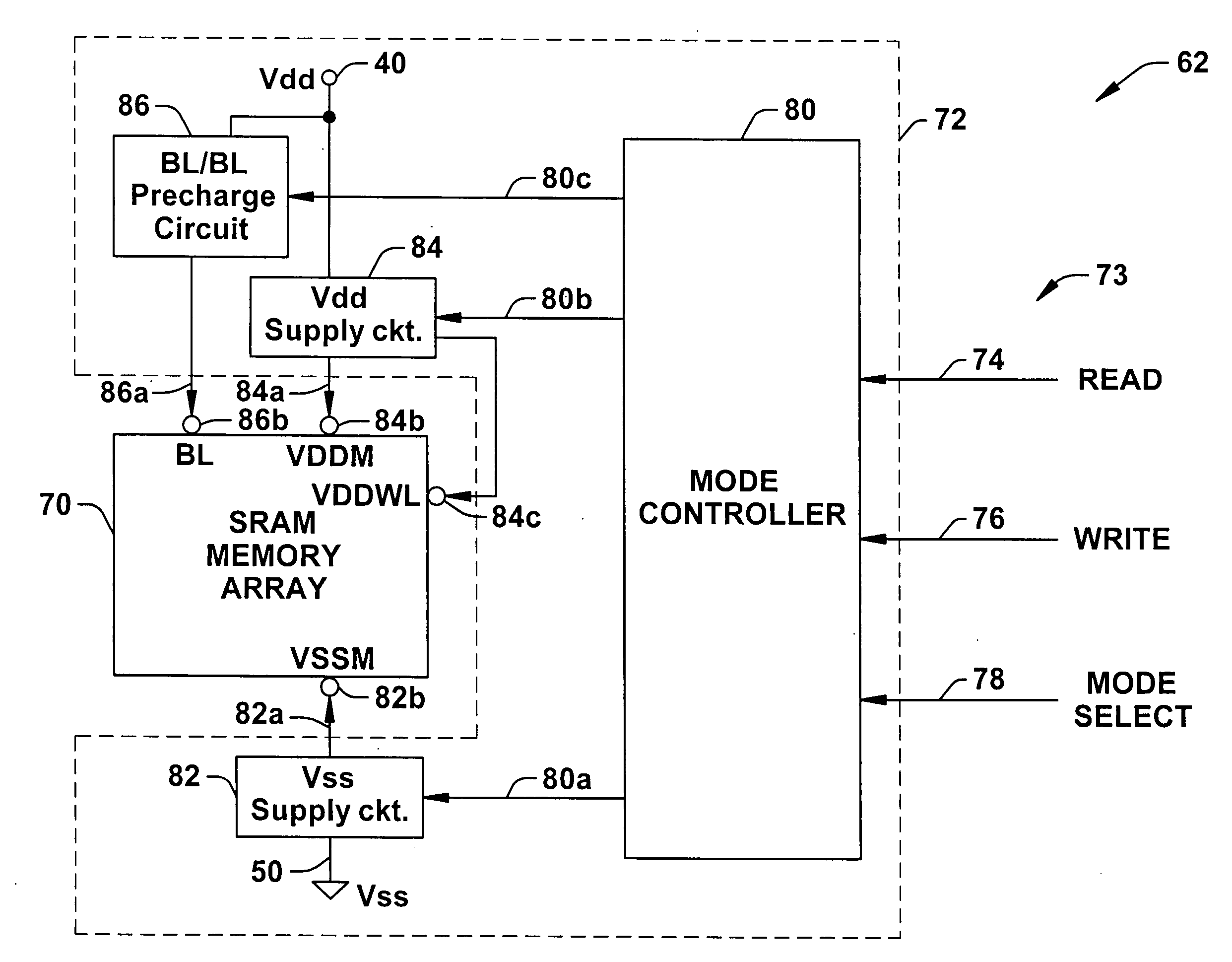
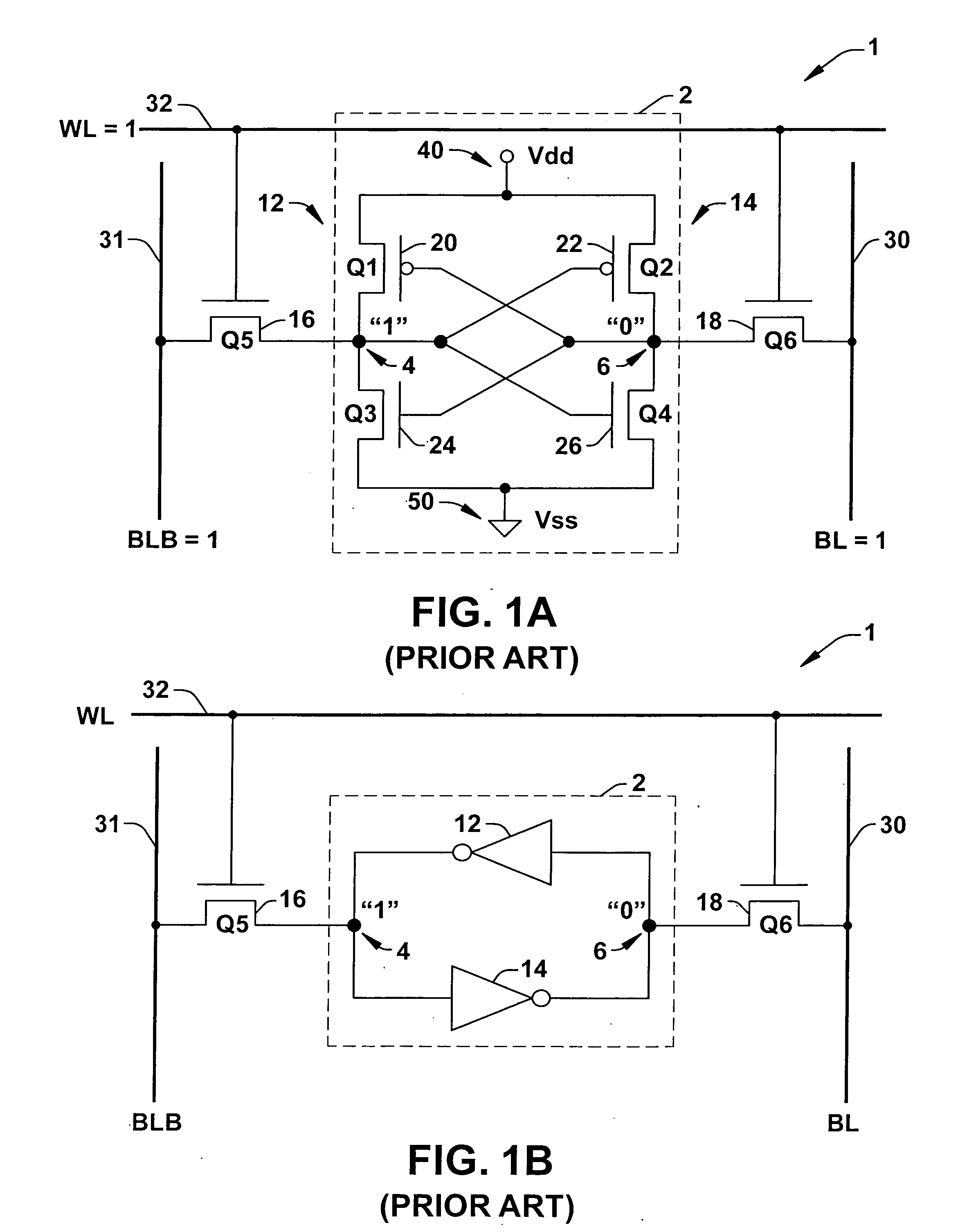
[0049]The present invention will now be described with reference to the attached drawings, wherein like reference numerals are used to refer to like elements throughout. The invention provides a memory array (e.g., an SRAM memory array), and / or a memory array embedded within an integrated circuit (IC), wherein the memory utilizes a new “low power WRITE” mode, mode control circuitry, and a method of implementing the same having a reduced IDDQ relative to the IDDQ of a full active mode (e.g., READ or WRITE mode). The new “low power WRITE” mode or “drowsy” mode is implemented by the mode control circuitry, which alters one or more supply and / or bitline precharge voltages of the memory array. These voltage alterations enable the low power WRITE mode, in one embodiment, to be intermediately biased between a “full active” mode, which permits READ and WRITE operations, and a “retention” mode that allows neither READ or WRITE operations. The low power WRITE mode permits a WRITE operation wh...


PUM


Abstract

The present invention describes circuitry and a method of providing a low power WRITE mode of operation for an integrated circuit comprising an SRAM memory to provide a reduced IDDQ relative to the IDDQ of a full active mode. In one aspect, the circuitry includes an SRAM memory array, mode control circuitry coupled to the array and configured to alter a supply voltage level to the SRAM array based on a mode of operation. The circuitry also includes control inputs coupled to the mode control circuitry for selecting one of the low power write mode, the full active mode, and optionally a retention mode of operation. The mode control circuitry is configured to receive the control inputs to select one of the three modes of operation, and to alter one or more supply voltage levels to the array, for example, the Vss supply voltage using a Vss supply circuit and the Vdd supply voltage using a Vdd supply circuit, based on the selected mode of operation. The mode control circuitry may also comprise a bitline precharge circuit configured to alter a bitline precharge voltage.

Description

FIELD OF INVENTION[0001]The present invention relates generally to semiconductor memory devices, and more particularly to an improved SRAM memory device comprising a WRITE mode having a reduced IDDQ relative to the IDDQ of a full active mode that reduces the leakage current, and minimizes latency and switching power overhead in embedded memory devices during write operations.BACKGROUND OF THE INVENTION[0002]Current trends in the semiconductor and electronics industry require memory devices to be made smaller, faster and require less power consumption. One reason for these trends is that more personal devices are being manufactured that are relatively small and portable, thereby relying on battery power. In addition to being smaller and more portable, personal devices are also requiring increased memory and more computational power and speed. In light of all these trends, there is an ever increasing demand in the industry for smaller, faster, and lower power dissipation memory cells ...

Claims


Application Information

Patent Timeline
IPC IPC(8): G11C5/14G11C11/00
CPCG11C11/413
Inventor HOUSTON, THEODORE WARRENCLINTON, MICHAEL PATRICKSHEFFIELD, BRYAN DAVID
Owner TEXAS INSTR INC
Why Eureka
Try Eureka