Apparatus and method for fabricating semiconductor device and removing by-products

a technology of semiconductor devices and by-products, which is applied in the direction of chemical apparatus and processes, coatings, coatings, etc., can solve the problems of short heating jacket lifetime, high price of heating jackets, and short effective life of vacuum pumps

Inactive Publication Date: 2008-03-06
DONGBU HITEK CO LTD
View PDF3 Cites 10 Cited by
  • Summary
  • Abstract
  • Description
  • Claims
  • Application Information

AI Technical Summary

Problems solved by technology

The by-products deposited on the foreline may cause various problems during processes performed in the process chamber.
For example, the by-products deposited on the inner wall of the foreline may flow back to the process chamber due to an abnormal pressure generated in the foreline or the process chamber.
Also, such by-products may have an effect on a vacuum pump for evacuating exhaust gas, such that an e

Method used


Image

  • Apparatus and method for fabricating semiconductor device and removing by-products
  • Apparatus and method for fabricating semiconductor device and removing by-products

Examples


Embodiment Construction

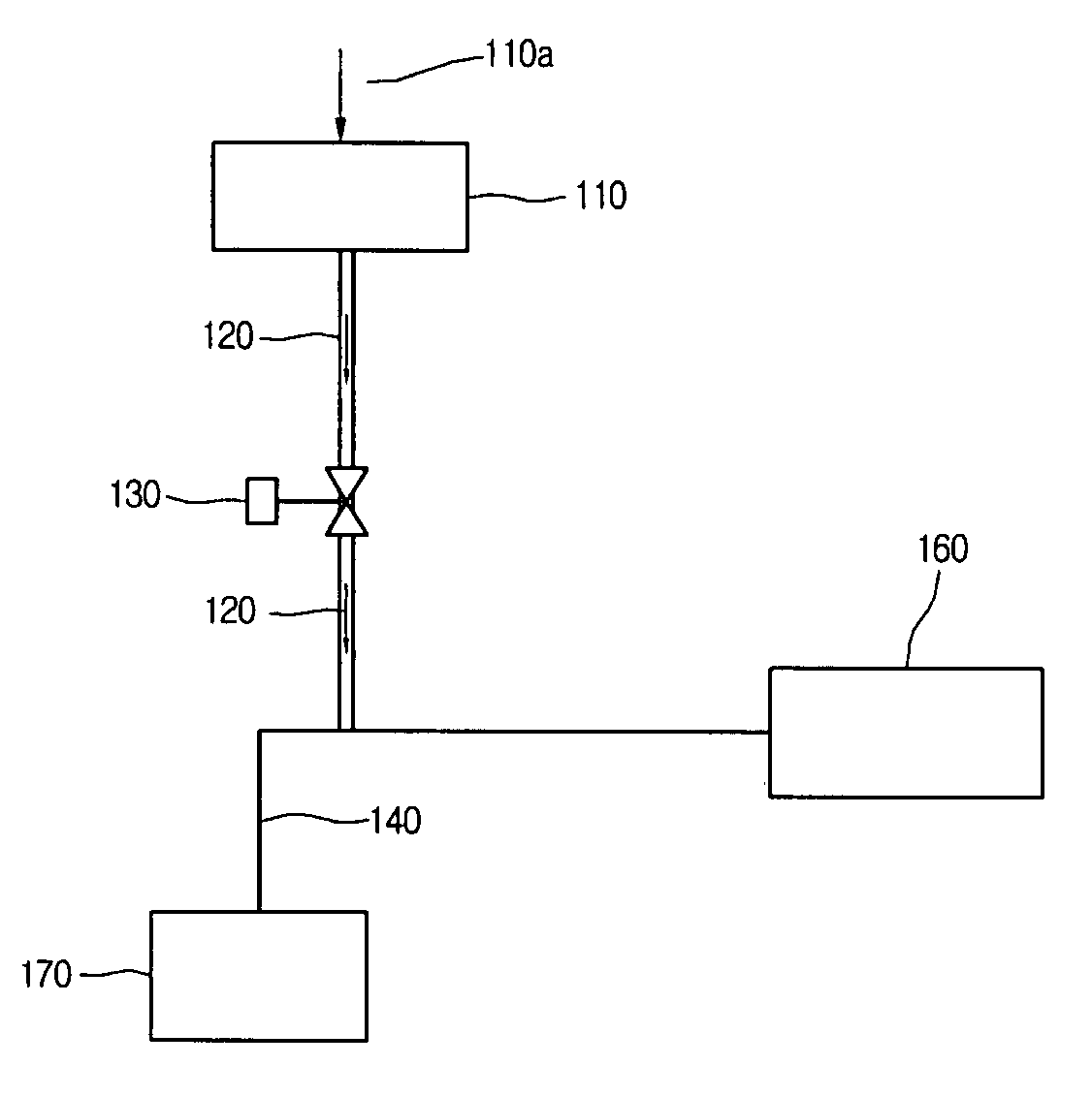
[0013]Hereinafter, an apparatus for fabricating a semiconductor device consistent with the present invention will be described in detail with reference to the accompanying drawings.

[0014]As shown in FIG. 1, the apparatus may comprise a chamber 170, where a semiconductor processing step may be performed; a foreline 140 for evacuating an exhaust gas; a pump 160 for evacuating the exhaust gas via foreline 140 from chamber 170.

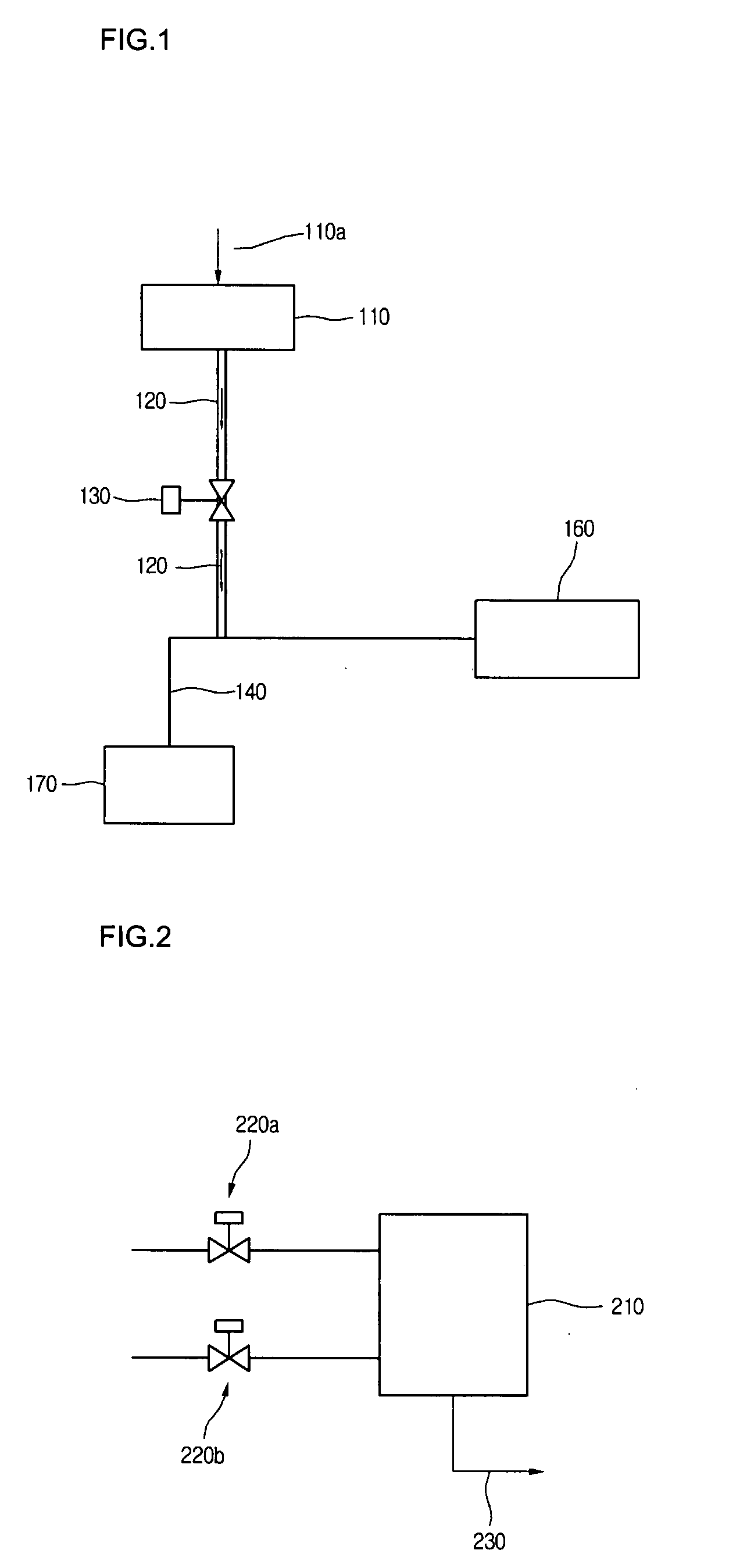
[0015]The apparatus may further comprise a remote plasma source 110 for providing plasma gas to foreline 140. Remote plasma source 110 may generate plasma by various means, for example, by using radio frequency electromagnetic waves. Remote plasma source 110 may comprise a gas inlet line 110a to provide a source gas to remote plasma source 110, and a plasma inlet line 120 to provide the plasma gas generated from remote plasma source 110 to foreline 140.

[0016]In one embodiment, the source gas may react with the by-products formed on the inner wall of foreline 140 t...


PUM

PropertyMeasurementUnit
Timeaaaaaaaaaa
Plasma poweraaaaaaaaaa

Abstract

An apparatus and a method for fabricating a semiconductor device are provided. The method can efficiently remove by-products from a foreline connected to a process chamber. The apparatus includes a remote plasma source, which generates a plasma gas. The plasma gas is guided to the foreline, so as to remove impurities formed on an inner wall of the foreline.

Description

[0001]The present application claims the benefit of priority under 35 U.S.C. §119 to Korean Patent Application No. 10-2006-0082398 (filed on Aug. 29, 2006), the entire contents of which are incorporated herein by reference.BACKGROUND[0002]1. Technical Field[0003]The present invention relates to a method and an apparatus for fabricating a semiconductor device. More specifically, the present invention relates to a method and an apparatus for fabricating a semiconductor device, and for efficiently removing by-products from a foreline to improve fabrication yield of the semiconductor device.[0004]2. Related Art[0005]Generally, by-products and / or active chemical species generated in a process chamber, where various processes may be performed, are exhausted through a foreline connected to the chamber. In the related art, the foreline may be made of a metallic material, such as aluminum (Al), stainless steel, etc. However, for such a metallic foreline, after a process, such as an etch proc...

Claims


Application Information

Patent Timeline
IPC IPC(8): H01L21/461C25F1/00H01L21/306
CPCC23C16/4405C23C16/4402H01L21/02
Inventor KIM, IN JUN
Owner DONGBU HITEK CO LTD
Why Eureka
Try Eureka