Semiconductor device
a technology of semiconductor devices and shielding rings, applied in semiconductor devices, semiconductor/solid-state device details, electrical devices, etc., can solve problems such as blockage regions not always provided along the sealing ring, and failure to meet the requirements of sealing ring requirements, so as to achieve the effect of suppressing noise transmission
- Summary
- Abstract
- Description
- Claims
- Application Information
AI Technical Summary
Benefits of technology
Problems solved by technology
Method used
Image

Examples
first embodiment
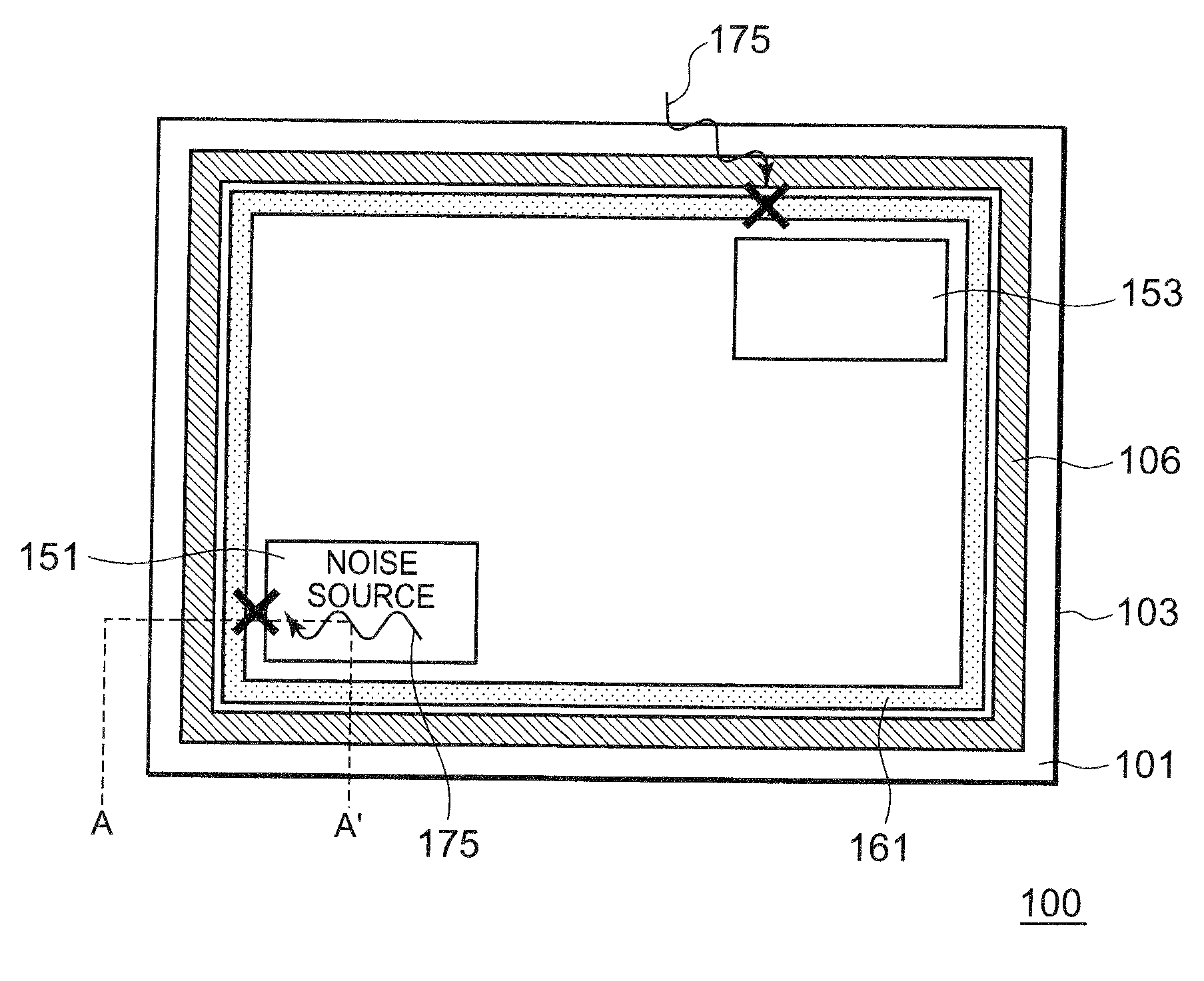
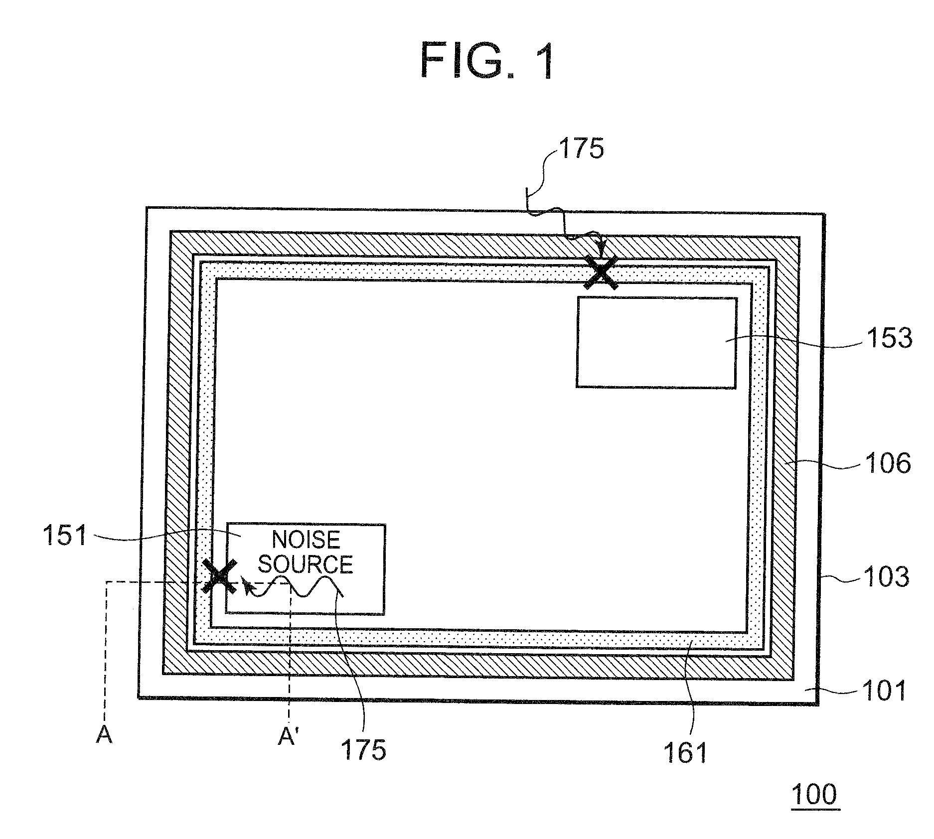
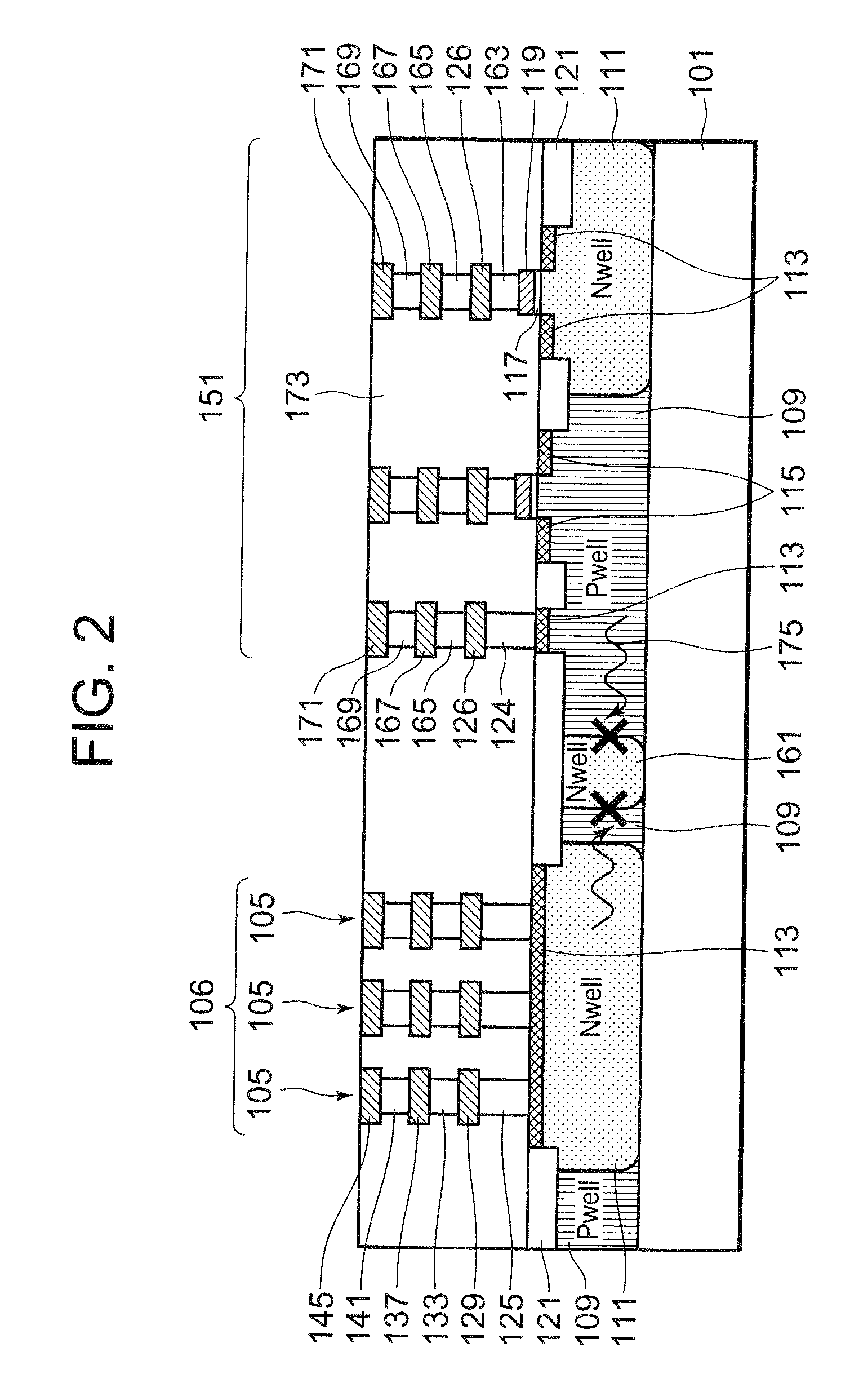
[0045]FIG. 1 shows a schematic top view of a configuration of a semiconductor device in this first embodiment. FIG. 2 shows a cross sectional view taken on line A-A′ of the semiconductor device 100 shown in FIG. 1. In FIG. 2 is shown a configuration of a seal ring region 106 and an internal circuit of a logic unit 151 provided inside the seal ring region 106. The cross section of an analog unit 153 is the same as, for example, that of the logic unit 151.
[0046]The semiconductor device 100 shown in FIGS. 1 and 2 respectively includes a first device region (logic unit 151) and a second device region (analog unit 153). The logic unit 151 is device region that might become a source of noise 175 and the analog unit 153 is a device region that might become a damaged circuit.
[0047]The semiconductor device 100 includes a semiconductor substrate (silicon substrate 101), an insulating interlayer 173 provided on the silicon substrate 101, and a conductive film buried in the insulating interlaye...
second embodiment
[0082]In the semiconductor device 100 in the first embodiment, the noise blocking region is constituted by one N well guard ring 161. However, the number of N well guard rings is not limited especially in this second embodiment; for example, plural N well guard rings may be disposed in a concentric pattern in the plane of the substrate. Hereunder, there will be described this second embodiment that will take such a configuration.
[0083]FIG. 3 shows a cross sectional view of a configuration of a semiconductor device in this second embodiment. Basically, the configuration is the same as that of the semiconductor device shown in FIG. 2 except that a first N well guard ring 177, a second N well guard ring 179, and a third N well guard ring 181 are provided instead of the N well guard ring 161. Also in this second embodiment, the cross sectional configuration of the analog unit 153 is the same as, for example, that of the logic unit 151.
[0084]Each of the first N well guard ring 177, the s...
third embodiment
[0090]FIG. 5 shows a cross sectional view of a configuration of a semiconductor device in this third embodiment. Basically, the configuration of the semiconductor device shown in FIG. 5 is the same as that shown in FIG. 2 except that the N well guard ring 161 that constitute a blocking region is fixed at a predetermined potential. In FIG. 5, the N+ diffusion layer 193 is provided near the surface of the silicon substrate 101 over the N well guard ring 161. In FIG. 5, the insulating interlayer 173 is omitted. Also in this third embodiment, the cross sectional configuration of the analog unit 153 is the same as, for example, that of the logic unit 151.
[0091]The N+ diffusion layer 193 may be formed over the forming region of the N well guard ring 161 entirely. It is also possible to form the layer 193 in part of the N well guard ring forming region. The planar shape of the N+ diffusion layer 193 may also be changed to, for example, a ring-like shape. The outer periphery of a side surfa...
PUM
 Abstract
Description
Claims
Application Information
 - R&D
- Intellectual Property
- Life Sciences
- Materials
- Tech Scout
- Unparalleled Data Quality
- Higher Quality Content
- 60% Fewer Hallucinations
Browse by: Latest US Patents, China's latest patents, Technical Efficacy Thesaurus, Application Domain, Technology Topic, Popular Technical Reports.
© 2025 PatSnap. All rights reserved.Legal|Privacy policy|Modern Slavery Act Transparency Statement|Sitemap|About US| Contact US: help@patsnap.com