Semiconductor device package and manufacturing method

a technology of semiconductor devices and manufacturing methods, applied in semiconductor devices, semiconductor/solid-state device details, electrical apparatus, etc., can solve problems such as noise, electromagnetic interference (emi) is the generation of undesired electrical signals, and affect the performance of circuitry,

Active Publication Date: 2008-03-13
ADVANCED SEMICON ENG INC
View PDF12 Cites 60 Cited by
  • Summary
  • Abstract
  • Description
  • Claims
  • Application Information

AI Technical Summary

Problems solved by technology

Semiconductor device packages typically have electrical circuitry implemented on a circuit substrate, such as a printed circuit board or a ceramic substrate The performance of the circuitry may be adversely affected by electromagnetic interference (EMI).
Electromagnetic interference (EMI) is the generation of undesired electrical signals, or noise, in electronic system circuitry due to the unintentional coupling of impinging electromagnetic field energy.
At the same time, the operating frequency of these electrical systems is increasing, further favoring the incidence of high frequency EMI.
The additive effect of all these sources of noise is to degrade the performance, or to induce errors in sensitive systems.

Method used


Image

  • Semiconductor device package and manufacturing method
  • Semiconductor device package and manufacturing method
  • Semiconductor device package and manufacturing method

Examples


Embodiment Construction

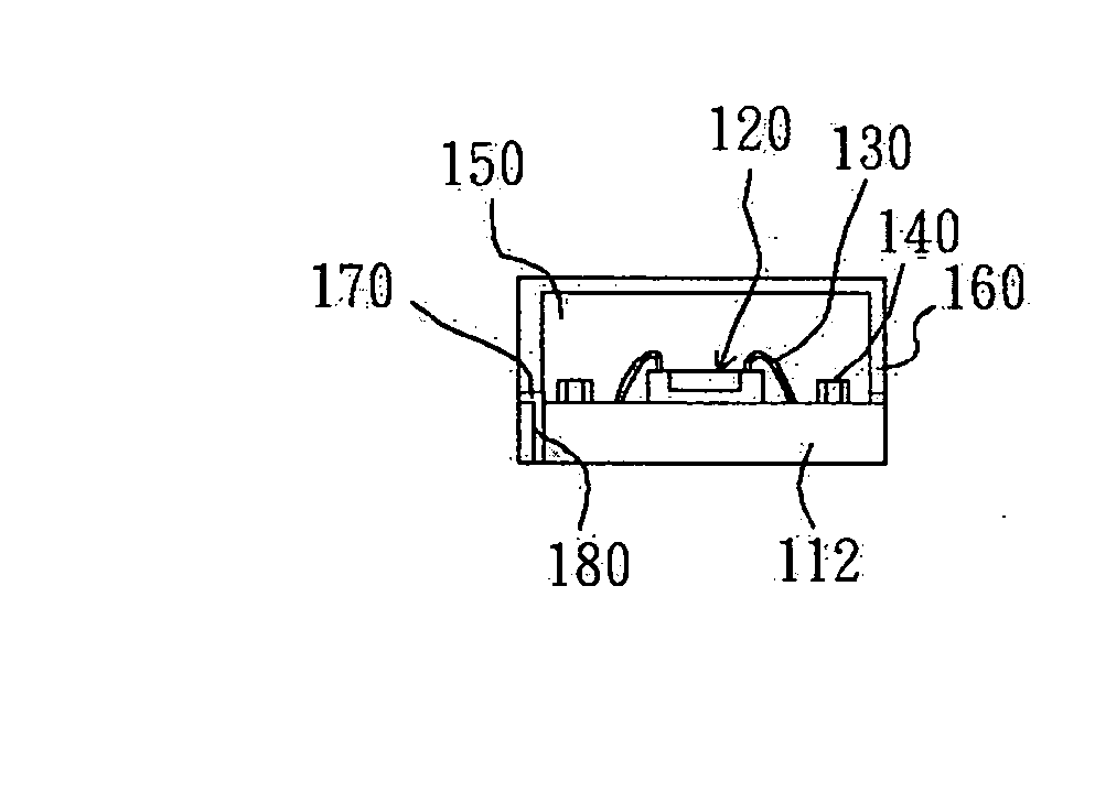
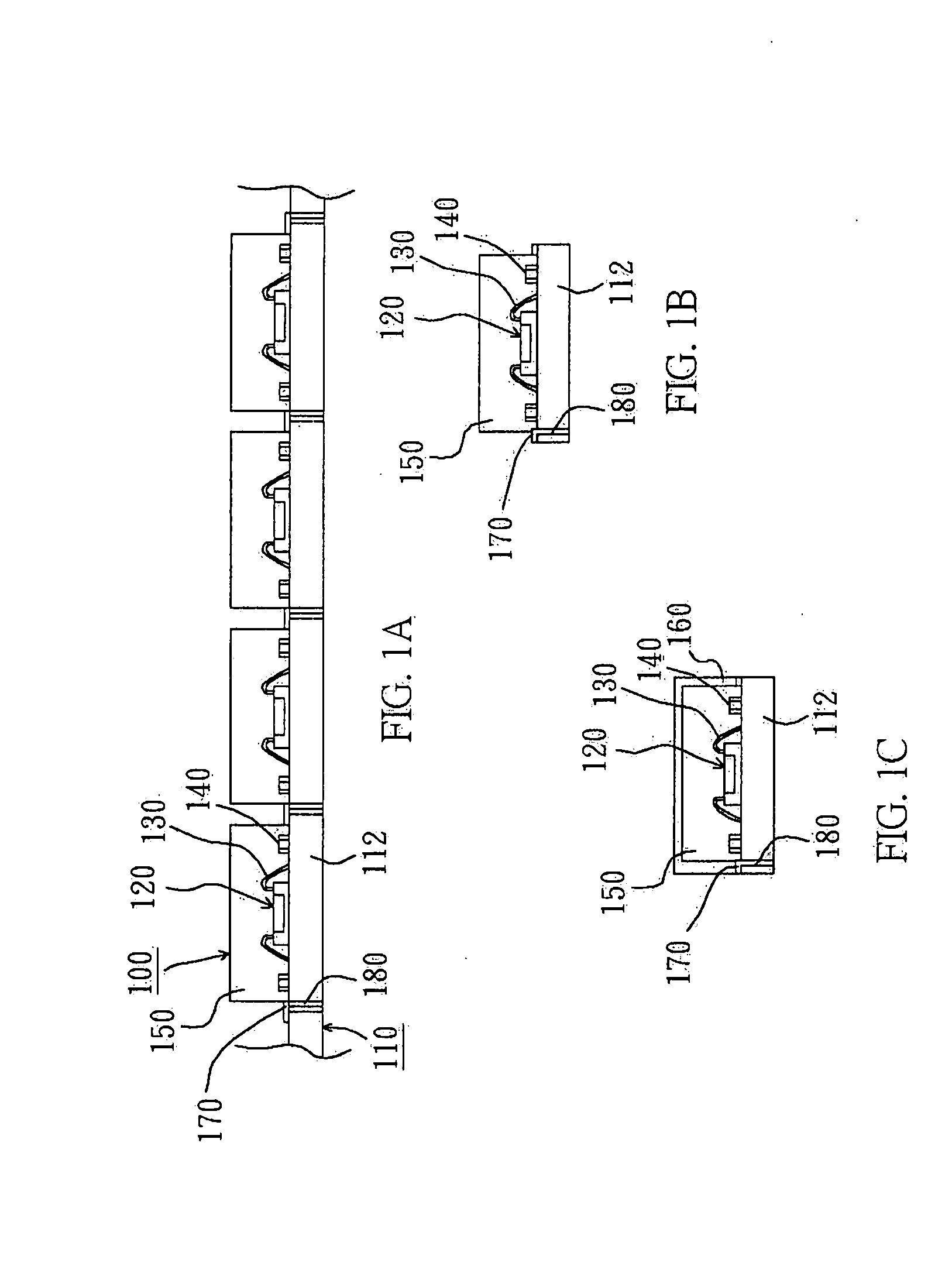
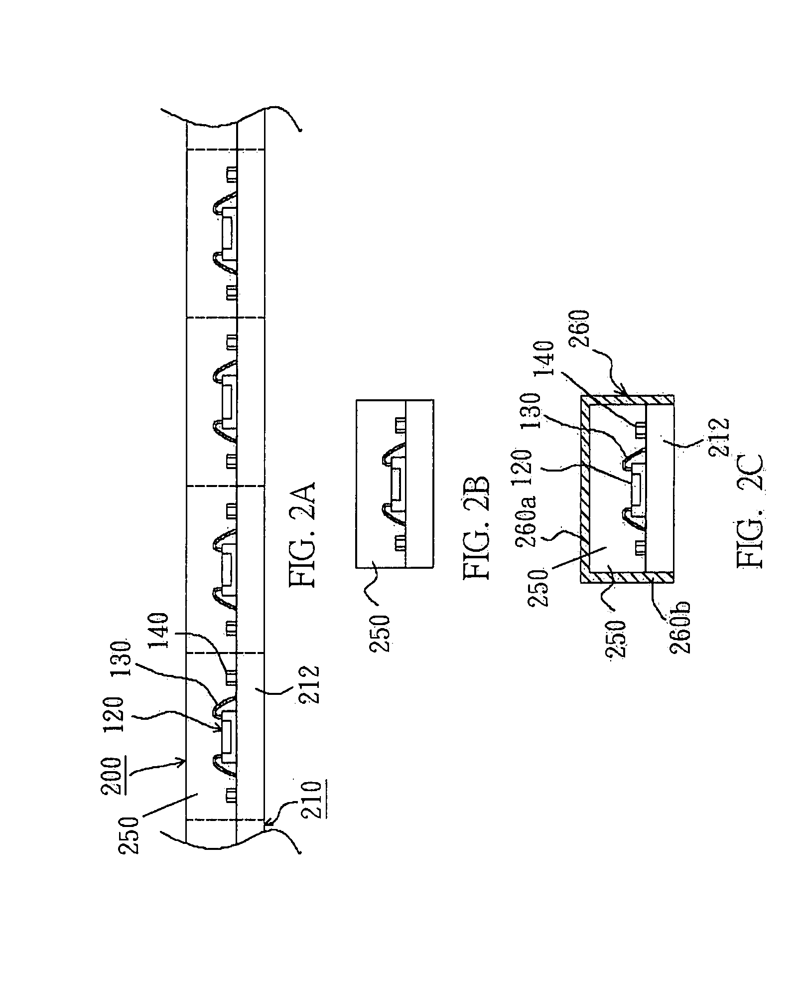
[0022]FIG. 1A to FIG. 1C illustrate a process for making a semiconductor device package according to one embodiment of the present invention.

[0023]FIG. 1A shows four molded products 100 (only one is denoted in FIG. 1A) provided on a substrate strip 110. The substrate strip 110 comprises a plurality of substrates 112 (only one is denoted in FIG. 1A). Though only four substrates 112 are shown in FIG. 1A, a substrate strip for use with the invention can include any numbers of substrates that is compatible with the manufacturing equipment, e.g., mold, being used. Each of the molded product 100 includes at least one semiconductor device 120 attached to a substrate 112 by means of a conductive adhesive (not shown) such as a silver-filled epoxy or a non-conductive adhesive (not shown). The semiconductor device 120 is connected to the substrate 112 by a plurality of bonding wires 130 which act as electrical input / output (I / O) connections to a first set of contacts (not shown), e.g., conduc...


PUM


Abstract

A semiconductor device package includes a semiconductor device mounted and electrically coupled to a substrate, a package body encapsulating the semiconductor device against a portion of an upper surface of the substrate; and an electromagnetic interference shielding layer formed over the package body and substantially enclosing the semiconductor device. The present invention further provides methods for manufacturing the semiconductor device package

Description

[0001] This application is a Divisional of co-pending application Ser. No. 11 / 028,670 filed on Jan. 5, 2005, the entire contents of which are hereby incorporated by reference and for which priority is claimed under 35 U.S.C §120.BACKGROUND OF THE INVENTION [0002] 1. Field of the Invention [0003] This invention relates to semiconductor device packages, and more specifically to semiconductor device packages which are shielded to protect against electromagnetic interference (EMI). [0004] 2. Description of the Related Art [0005] Semiconductor device packages typically have electrical circuitry implemented on a circuit substrate, such as a printed circuit board or a ceramic substrate The performance of the circuitry may be adversely affected by electromagnetic interference (EMI). Electromagnetic interference (EMI) is the generation of undesired electrical signals, or noise, in electronic system circuitry due to the unintentional coupling of impinging electromagnetic field energy. [0006] ...

Claims


Application Information

Patent Timeline
Patent Type & Authority Applications(United States)
IPC IPC(8): H01L23/552H01L21/60
CPCH01L21/561H01L23/29H01L2924/07802H01L2924/01087H01L2924/01033H01L2924/01006H01L2924/01005H01L23/3121H01L23/3135H01L23/552H01L24/97H01L2224/48091H01L2224/48227H01L2224/97H01L2924/01002H01L2924/01027H01L2924/01029H01L2924/01047H01L2924/01079H01L2924/16152H01L2924/19105H01L2924/3011H01L2924/3025H01L24/48H01L2224/85H01L2924/00014H01L2924/00H01L2924/15787H01L2924/181H01L2924/00012H01L2224/45099H01L2224/45015H01L2924/207
Inventor YANG, JUN YOUNGJOO, YOU OCKJUNG, DONG PIL
Owner ADVANCED SEMICON ENG INC
Why Eureka
Try Eureka